SNVS346G November 2007 – November 2023 LM3481
PRODUCTION DATA
- 1
- 1 Features
- 2 Applications
- 3 Description
- 4 Pin Configuration and Functions
- 5 Specifications
- 6 Detailed Description
-
7 Application and Implementation
- 7.1 Application Information
- 7.2
Typical Applications
- 7.2.1
Boost Converter
- 7.2.1.1 Design Requirements
- 7.2.1.2
Detailed Design Procedure
- 7.2.1.2.1 Custom Design with WEBENCH Tools
- 7.2.1.2.2 Power Inductor Selection
- 7.2.1.2.3 Programming the Output Voltage and Output Current
- 7.2.1.2.4 Current Limit With Additional Slope Compensation
- 7.2.1.2.5 Power Diode Selection
- 7.2.1.2.6 Power MOSFET Selection
- 7.2.1.2.7 Input Capacitor Selection
- 7.2.1.2.8 Output Capacitor Selection
- 7.2.1.2.9 Driver Supply Capacitor Selection
- 7.2.1.2.10 Compensation
- 7.2.1.3 Application Curve
- 7.2.2 Typical SEPIC Converter
- 7.2.1
Boost Converter
- 7.3 Power Supply Recommendations
- 7.4 Layout
- 8 Device and Documentation Support
- 9 Revision History
- 10Mechanical, Packaging, and Orderable Information
Package Options
Mechanical Data (Package|Pins)
- DGS|10
Thermal pad, mechanical data (Package|Pins)
Orderable Information
7.2.1.2.4 Current Limit With Additional Slope Compensation
If an external slope compensation resistor is used (see Figure 6-6) the internal control signal will be modified and this will have an effect on the current limit.
If RSL is used, then this will add to the existing slope compensation. The command voltage, VCS, will then be given by:
Where VSENSE is a defined parameter in the Electrical CharacteristicsElectrical CharacteristicsElectrical Characteristics section and ΔVSL is the additional slope compensation generated as discussed in the Section 6.3.3 section. This changes the equation for RSEN to:
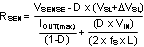
Note that because ΔVSL = RSL x K as defined earlier, RSLcan be used to provide an additional method for setting the current limit. In some designs RSL can also be used to help filter noise to keep the ISEN pin quiet.