SNVS424D January 2006 – December 2014 LM5106
PRODUCTION DATA.
- 1 Features
- 2 Applications
- 3 Description
- 4 Revision History
- 5 Pin Configuration and Functions
- 6 Specifications
- 7 Detailed Description
- 8 Application and Implementation
- 9 Power Supply Recommendations
- 10Layout
- 11Device and Documentation Support
- 12Mechanical, Packaging, and Orderable Information
Package Options
Mechanical Data (Package|Pins)
Thermal pad, mechanical data (Package|Pins)
Orderable Information
10 Layout
10.1 Layout Guidelines
The optimum performance of high- and low-side gate drivers cannot be achieved without taking due considerations during circuit board layout. The following points are emphasized:
- Low ESR / ESL capacitors must be connected close to the IC between VDD and VSS pins and between HB and HS pins to support high peak currents being drawn from VDD and HB during the turnon of the external MOSFETs.
- To prevent large voltage transients at the drain of the top MOSFET, a low ESR electrolytic capacitor and a good quality ceramic capacitor must be connected between the MOSFET drain and ground (VSS).
- To avoid large negative transients on the switch node (HS) pin, the parasitic inductances between the source of the top MOSFET and the drain of the bottom MOSFET (synchronous rectifier) must be minimized.
- Grounding considerations:
- The first priority in designing grounding connections is to confine the high peak currents that charge and discharge the MOSFET gates to a minimal physical area. This will decrease the loop inductance and minimize noise issues on the gate terminals of the MOSFETs. The gate driver should be placed as close as possible to the MOSFETs.
- The second consideration is the high current path that includes the bootstrap capacitor, the bootstrap diode, the local ground referenced bypass capacitor, and the low-side MOSFET body diode. The bootstrap capacitor is recharged on a cycle-by-cycle basis through the bootstrap diode from the ground referenced VDD bypass capacitor. The recharging occurs in a short time interval and involves high peak current. Minimizing this loop length and area on the circuit board is important to ensure reliable operation.
- The resistor on the RDT pin must be placed very close to the IC and separated from the high current paths to avoid noise coupling to the time delay generator which could disrupt timer operation.
10.1.1 HS Transient Voltages Below Ground
The HS node will always be clamped by the body diode of the lower external FET. In some situations, board resistances and inductances can cause the HS node to transiently swing several volts below ground. The HS node can swing below ground provided:
- HS must always be at a lower potential than HO. Pulling HO more than –0.3 V below HS can activate parasitic transistors resulting in excessive current flow from the HB supply, possibly resulting in damage to the IC. The same relationship is true with LO and VSS. If necessary, a Schottky diode can be placed externally between HO and HS or LO and GND to protect the IC from this type of transient. The diode must be placed as close to the IC pins as possible in order to be effective.
- HB to HS operating voltage should be 15 V or less. Hence, if the HS pin transient voltage is –5 V, VDD should be ideally limited to 10V to keep HB to HS below 15 V.
- Low ESR bypass capacitors from HB to HS and from VCC to VSS are essential for proper operation. The capacitor should be located at the leads of the IC to minimize series inductance. The peak currents from LO and HO can be quite large. Any inductances in series with the bypass capacitor will cause voltage ringing at the leads of the IC which must be avoided for reliable operation.
10.2 Layout Example
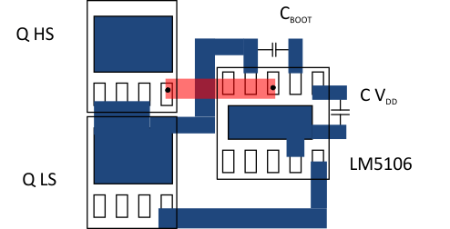 Figure 21. LM5106 Component Placement