SNVS424D January 2006 – December 2014 LM5106
PRODUCTION DATA.
- 1 Features
- 2 Applications
- 3 Description
- 4 Revision History
- 5 Pin Configuration and Functions
- 6 Specifications
- 7 Detailed Description
- 8 Application and Implementation
- 9 Power Supply Recommendations
- 10Layout
- 11Device and Documentation Support
- 12Mechanical, Packaging, and Orderable Information
Package Options
Mechanical Data (Package|Pins)
Thermal pad, mechanical data (Package|Pins)
Orderable Information
5 Pin Configuration and Functions
10-Pin
VSSOP (DGS), WSON (DPR)
Top View
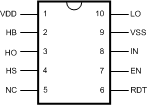
Pin Functions
| PIN | DESCRIPTION | APPLICATION INFORMATION | |
|---|---|---|---|
| NO. | NAME | ||
| 1 | VDD | Positive gate drive supply | Decouple VDD to VSS using a low ESR/ESL capacitor, placed as close to the IC as possible. |
| 2 | HB | High-side gate driver bootstrap rail | Connect the positive terminal of bootstrap capacitor to the HB pin and connect negative terminal to HS. The Bootstrap capacitor should be placed as close to IC as possible. |
| 3 | HO | High-side gate driver output | Connect to the gate of high-side N-MOS device through a short, low inductance path. |
| 4 | HS | High-side MOSFET source connection | Connect to the negative terminal of the bootststrap capacitor and to the source of the high-side N-MOS device. |
| 5 | NC | Not connected | |
| 6 | RDT | Dead-time programming pin | A resistor from RDT to VSS programs the turnon delay of both the high- and low-side MOSFETs. The resistor should be placed close to the IC to minimize noise coupling from adjacent PC board traces. |
| 7 | EN | Logic input for driver Disable/Enable | TTL compatible threshold with hysteresis. LO and HO are held in the low state when EN is low. |
| 8 | IN | Logic input for gate driver | TTL compatible threshold with hysteresis. The high-side MOSFET is turned on and the low-side MOSFET turned off when IN is high. |
| 9 | VSS | Ground return | All signals are referenced to this ground. |
| 10 | LO | Low-side gate driver output | Connect to the gate of the low-side N-MOS device with a short, low inductance path. |
| — | EP | Exposed Pad | The exposed pad has no electrical contact. Connect to system ground plane for reduced thermal resistance. |