SNVS676I August 2010 – April 2018 LM5119
PRODUCTION DATA.
- 1 Features
- 2 Applications
- 3 Description
- 4 Revision History
- 5 Pin Configuration and Functions
- 6 Specifications
-
7 Detailed Description
- 7.1 Overview
- 7.2 Functional Block Diagram
- 7.3
Feature Description
- 7.3.1 High Voltage Start-Up Regulator
- 7.3.2 UVLO
- 7.3.3 Enable 2
- 7.3.4 Oscillator and Sync Capability
- 7.3.5 Error Amplifiers and PWM Comparators
- 7.3.6 Ramp Generator
- 7.3.7 Current Limit
- 7.3.8 Hiccup Mode Current Limiting
- 7.3.9 Soft Start
- 7.3.10 HO and LO Output Drivers
- 7.3.11 Maximum Duty Cycle
- 7.3.12 Thermal Protection
- 7.4 Device Functional Modes
-
8 Application and Implementation
- 8.1 Application Information
- 8.2
Typical Applications
- 8.2.1
Dual-output Design Example
- 8.2.1.1 Design Requirements
- 8.2.1.2
Detailed Design Procedure
- 8.2.1.2.1 Timing Resistor
- 8.2.1.2.2 Output Inductor
- 8.2.1.2.3 Current Sense Resistor
- 8.2.1.2.4 Ramp Resistor and Ramp Capacitor
- 8.2.1.2.5 Output Capacitors
- 8.2.1.2.6 Input Capacitors
- 8.2.1.2.7 VCC Capacitor
- 8.2.1.2.8 Bootstrap Capacitor
- 8.2.1.2.9 Soft-Start Capacitor
- 8.2.1.2.10 Restart Capacitor
- 8.2.1.2.11 Output Voltage Divider
- 8.2.1.2.12 UVLO Divider
- 8.2.1.2.13 MOSFET Snubber
- 8.2.1.2.14 Error Amplifier Compensation
- 8.2.1.3 Application Curves
- 8.2.2 Two-Phase Design Example
- 8.2.1
Dual-output Design Example
- 9 Power Supply Recommendations
- 10Layout
- 11Device and Documentation Support
- 12Mechanical, Packaging, and Orderable Information
Package Options
Mechanical Data (Package|Pins)
- RTV|32
Thermal pad, mechanical data (Package|Pins)
- RTV|32
Orderable Information
8.2.1.2.11 Output Voltage Divider
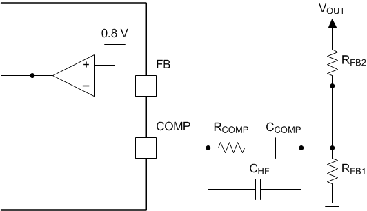
RFB1 and RFB2 set the output voltage level, the ratio of these resistors is calculated from Equation 33.
Equation 33. 

1.33 kΩ was chosen for RFB1 in this design which results in a RFB2 value of 6.98 kΩ for VOUT2 of 5 V. A reasonable guide is to select the value of RFB1 in the range between 500 Ω and 10 kΩ. The value of RFB1 must be large enough to keep the total divider power dissipation small.
 Figure 16. Feedback Configuration