SNVS808C May 2012 – Februrary 2016 LM5134
PRODUCTION DATA.
- 1 Features
- 2 Applications
- 3 Description
- 4 Revision History
- 5 Pin Configuration and Functions
- 6 Specifications
- 7 Detailed Description
- 8 Application and Implementation
- 9 Power Supply Recommendations
- 10Layout
- 11Device and Documentation Support
- 12Mechanical, Packaging, and Orderable Information
Package Options
Mechanical Data (Package|Pins)
Thermal pad, mechanical data (Package|Pins)
Orderable Information
1 Features
- 7.6-A and 4.5-A Peak Sink and Source Drive Current for Main Output
- 820-mA and 660-mA Peak Sink and Source Current for PILOT Output
- 4-V to 12.6-V Single-Power Supply
- Matching Delay Time Between Inverting and Non-Inverting Inputs
- TTL/CMOS Logic Inputs
- Up to 14-V Logic Inputs (Regardless of VDD Voltage)
- –40°C to 125°C Junction Temperature Range
2 Applications
- Motor Drivers
- Solid-State Power Controllers
- Power Factor Correction Converters
3 Description
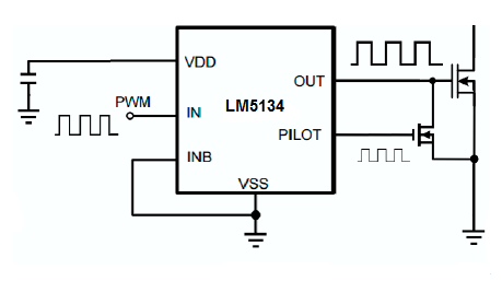
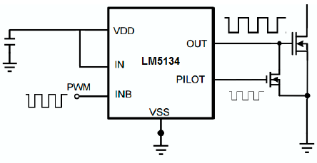
The LM5134 is a high-speed single low-side driver capable of sinking and sourcing 7.6-A and 4.5-A peak currents. The LM5134 has inverting and noninverting inputs that give the user greater flexibility in controlling the FET. The LM5134 features one main output, OUT, and an extra gate drive output, PILOT. The PILOT pin logic is complementary to the OUT pin, and can be used to drive a small MOSFET located close to the main power FET. This configuration minimizes the turnoff loop and reduces the consequent parasitic inductance. It is particularly useful for driving high-speed FETs or multiple FETs in parallel. The LM5134 is available in the 6-pin
SOT-23 package and the 6-pin WSON package with an exposed pad to aid thermal dissipation.
Device Information(1)
| PART NUMBER | PACKAGE | BODY SIZE (NOM) |
|---|---|---|
| LM5134 | SOT-23 (6) | 2.90 mm × 1.60 mm |
| WSON (6) | 3.00 mm × 3.00 mm |
- For all available packages, see the orderable addendum at the end of the data sheet.
Noninverting Input

Inverting Input
