SNVSAZ0C March 2018 – October 2021 LM51501-Q1
PRODUCTION DATA
- 1 Features
- 2 Applications
- 3 Description
- 4 Revision History
- 5 Device Comparison Table
- 6 Pin Configuration and Functions
- 7 Specifications
-
8 Detailed Description
- 8.1 Overview
- 8.2 Functional Block Diagram
- 8.3
Feature Description
- 8.3.1 Enable (EN Pin)
- 8.3.2 High Voltage VCC Regulator (PVCC, AVCC Pin)
- 8.3.3 Power-On Voltage Selection (VSET Pin)
- 8.3.4 Switching Frequency (RT Pin)
- 8.3.5 Clock Synchronization (SYNC Pin in SS Configuration)
- 8.3.6 Current Sense, Slope Compensation, and PWM (CS Pin)
- 8.3.7 Current Limit (CS Pin)
- 8.3.8 Feedback and Error Amplifier (COMP Pin)
- 8.3.9 Automatic Wake-Up and Standby
- 8.3.10 Boost Status Indicator (STATUS Pin)
- 8.3.11 Maximum Duty Cycle Limit and Minimum Input Supply Voltage
- 8.3.12 MOSFET Driver (LO Pin)
- 8.3.13 Thermal Shutdown
- 8.4 Device Functional Modes
-
9 Application and Implementation
- 9.1 Application Information
- 9.2
Typical Application
- 9.2.1 Design Requirements
- 9.2.2
Detailed Design Procedure
- 9.2.2.1 Custom Design With WEBENCH® Tools
- 9.2.2.2 RSET Resistor
- 9.2.2.3 RT Resistor
- 9.2.2.4 Inductor Selection (LM)
- 9.2.2.5 Current Sense (RS)
- 9.2.2.6 Slope Compensation Ramp (RSL)
- 9.2.2.7 Output Capacitor (COUT)
- 9.2.2.8 Loop Compensation Component Selection and Maximum ESR
- 9.2.2.9 PVCC Capacitor, AVCC Capacitor, and AVCC Resistor
- 9.2.2.10 VOUT Filter (CVOUT, RVOUT)
- 9.2.2.11 Input Capacitor
- 9.2.2.12 MOSFET Selection
- 9.2.2.13 Diode Selection
- 9.2.2.14 Efficiency Estimation
- 9.2.3 Application Curves
- 9.3 System Examples
- 10Power Supply Recommendations
- 11Layout
- 12Device and Documentation Support
- 13Mechanical, Packaging, and Orderable Information
Package Options
Refer to the PDF data sheet for device specific package drawings
Mechanical Data (Package|Pins)
- RUM|16
Thermal pad, mechanical data (Package|Pins)
- RUM|16
Orderable Information
3 Description
The LM51501-Q1 is a wide input range automatic boost controller. The device can be used to maintain a stable output voltage during automotive cranking from a vehicle battery or from a backup battery.
The LM51501-Q1 switching frequency is programmed by a resistor from 220 kHz to 2.3 MHz. Fast switching (≥ 2.2 MHz) minimizes AM band interference and allows for a small solution size and fast transient response.
The LM51501-Q1 operates in low IQ standby mode when the input or output voltage is above the preset standby thresholds and automatically wakes up when the output voltage drops below the preset wake-up threshold.
The device transitions in and out of low IQ standby mode to extend battery life at light load. A single resistor programs the target output regulation voltage as well as the configuration. Additional features include low shutdown current, boost status indicator, adjustable cycle-by-cycle current limit, and thermal shutdown. A status indicator can be used to control a circuit to bypass the diode when the part is not boosting in order to reduce power dissipation. In E-call mode, the device can be used to control a disconnect switch to protect the backup-battery.
| PART NUMBER | PACKAGE(1) | BODY SIZE (NOM) |
|---|---|---|
| LM51501-Q1 | WQFN (16) | 4.00 mm × 4.00 mm |
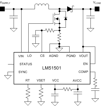
 Typical Application
Circuit
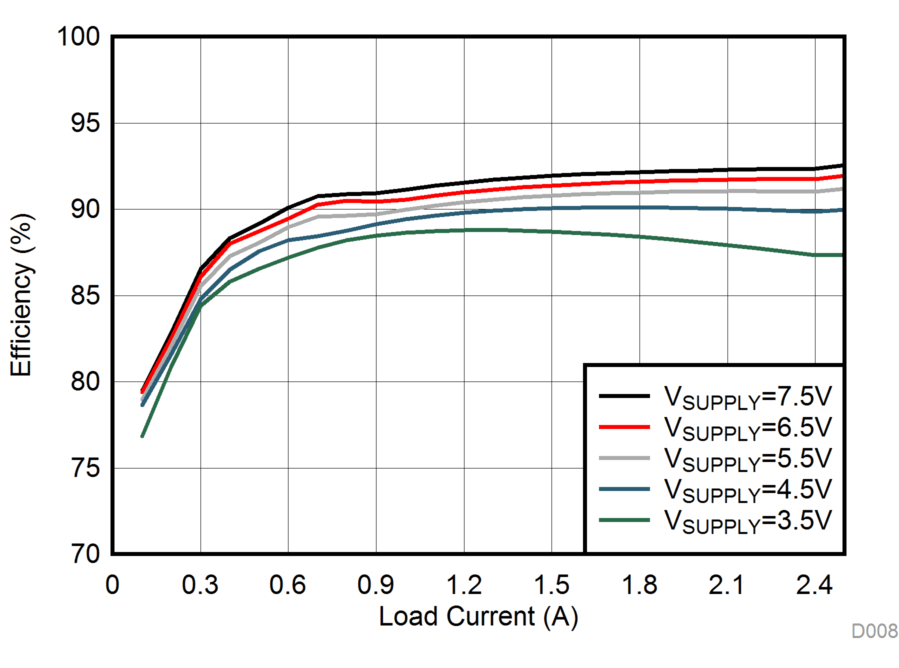
 Efficiency (VLOAD
= 9.5 V, FSW = 440 kHz)