SNOSBQ4F May   1999  – January 2022 LM567C

PRODUCTION DATA  

  1. Features
  2. Applications
  3. Description
  4. Revision History
  5. Device Comparison
  6. Pin Configuration and Functions
  7. Specifications
    1. 7.1 Absolute Maximum Ratings
    2. 7.2 Recommended Operating Conditions
    3. 7.3 Thermal Information
    4. 7.4 Electrical Characteristics
    5. 7.5 Typical Characteristics
  8. Parameter Measurement Information
  9. Detailed Description
    1. 9.1 Overview
    2. 9.2 Functional Block Diagram
    3. 9.3 Feature Description
      1. 9.3.1 Center Frequency
      2. 9.3.2 Output Filter
      3. 9.3.3 Loop Filter
      4. 9.3.4 Logic Output
      5. 9.3.5 Die Characteristics
    4. 9.4 Device Functional Modes
      1. 9.4.1 Operation With Vi < 200m – VRMS
      2. 9.4.2 Operation With Vi > 200m – VRMS
  10. 10Application and Implementation
    1. 10.1 Application Information
    2. 10.2 Typical Applications
      1. 10.2.1 Touch-Tone Decoder
        1. 10.2.1.1 Design Requirements
        2. 10.2.1.2 Detailed Design Procedure
          1. 10.2.1.2.1 Timing Components
          2. 10.2.1.2.2 Bandwidth
          3. 10.2.1.2.3 Output Filter
        3. 10.2.1.3 Application Curve
      2. 10.2.2 Oscillator with Quadrature Output
        1. 10.2.2.1 Design Requirements
        2. 10.2.2.2 Detailed Design Procedure
        3. 10.2.2.3 Application Curve
      3. 10.2.3 Oscillator with Double Frequency Output
        1. 10.2.3.1 Design Requirements
        2. 10.2.3.2 Detailed Design Procedure
        3. 10.2.3.3 Application Curve
      4. 10.2.4 Precision Oscillator Drive 100-mA Loads
        1. 10.2.4.1 Design Requirements
        2. 10.2.4.2 Detailed Design Procedure
        3. 10.2.4.3 Application Curve
      5. 10.2.5 AC Test Circuit
        1. 10.2.5.1 Design Requirements
        2. 10.2.5.2 Detailed Design Procedure
        3. 10.2.5.3 Application Curve
  11. 11Power Supply Recommendations
  12. 12Layout
    1. 12.1 Layout Guidelines
    2. 12.2 Layout Example
  13. 13Device and Documentation Support
    1. 13.1 Receiving Notification of Documentation Updates
    2. 13.2 Support Resources
    3. 13.3 Trademarks
    4. 13.4 Electrostatic Discharge Caution
    5. 13.5 Glossary
  14. 14Mechanical, Packaging, and Orderable Information

Package Options

Mechanical Data (Package|Pins)
Thermal pad, mechanical data (Package|Pins)
Orderable Information

Typical Characteristics

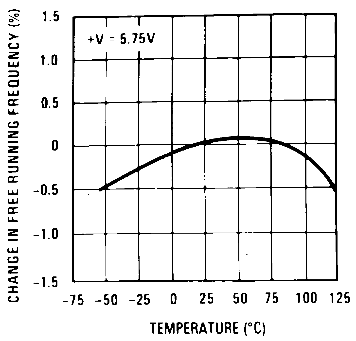
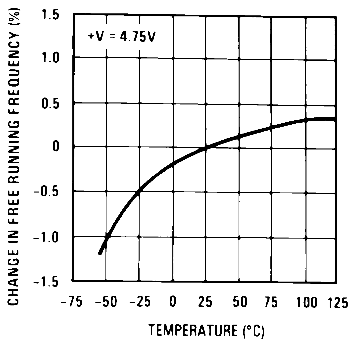
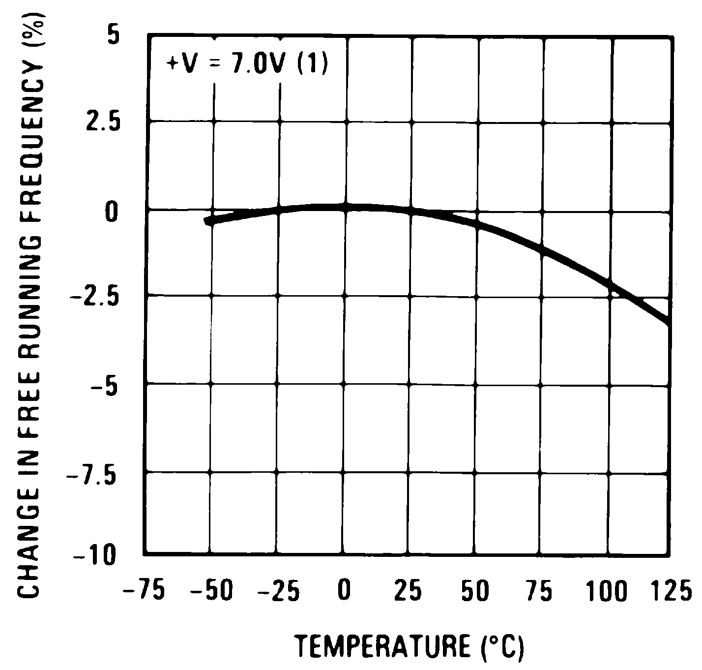
GUID-686EDE1F-90F5-472A-91C0-49E6AEFED48E-low.pngFigure 7-1 Typical Frequency Drift
GUID-FBD61630-4E5A-4A5B-A333-98DFC980388B-low.pngFigure 7-3 Typical Frequency Drift
GUID-6D1DA06E-CB63-4D9F-BDC5-E8DA2B33C584-low.pngFigure 7-5 Bandwidth vs Input Signal Amplitude
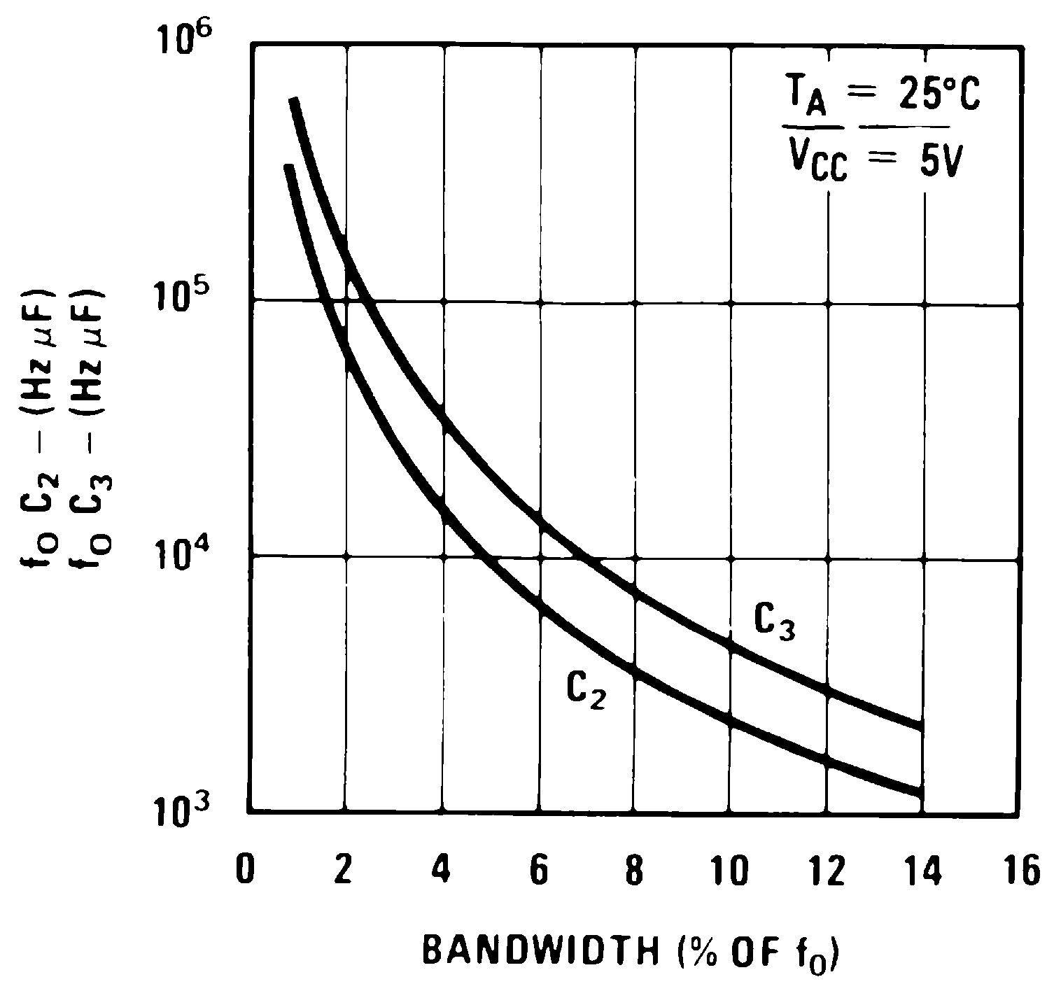
GUID-08476202-0F1F-4F76-9ECA-7D4585894059-low.pngFigure 7-7 Detection Bandwidth as a Function of C2 and C3
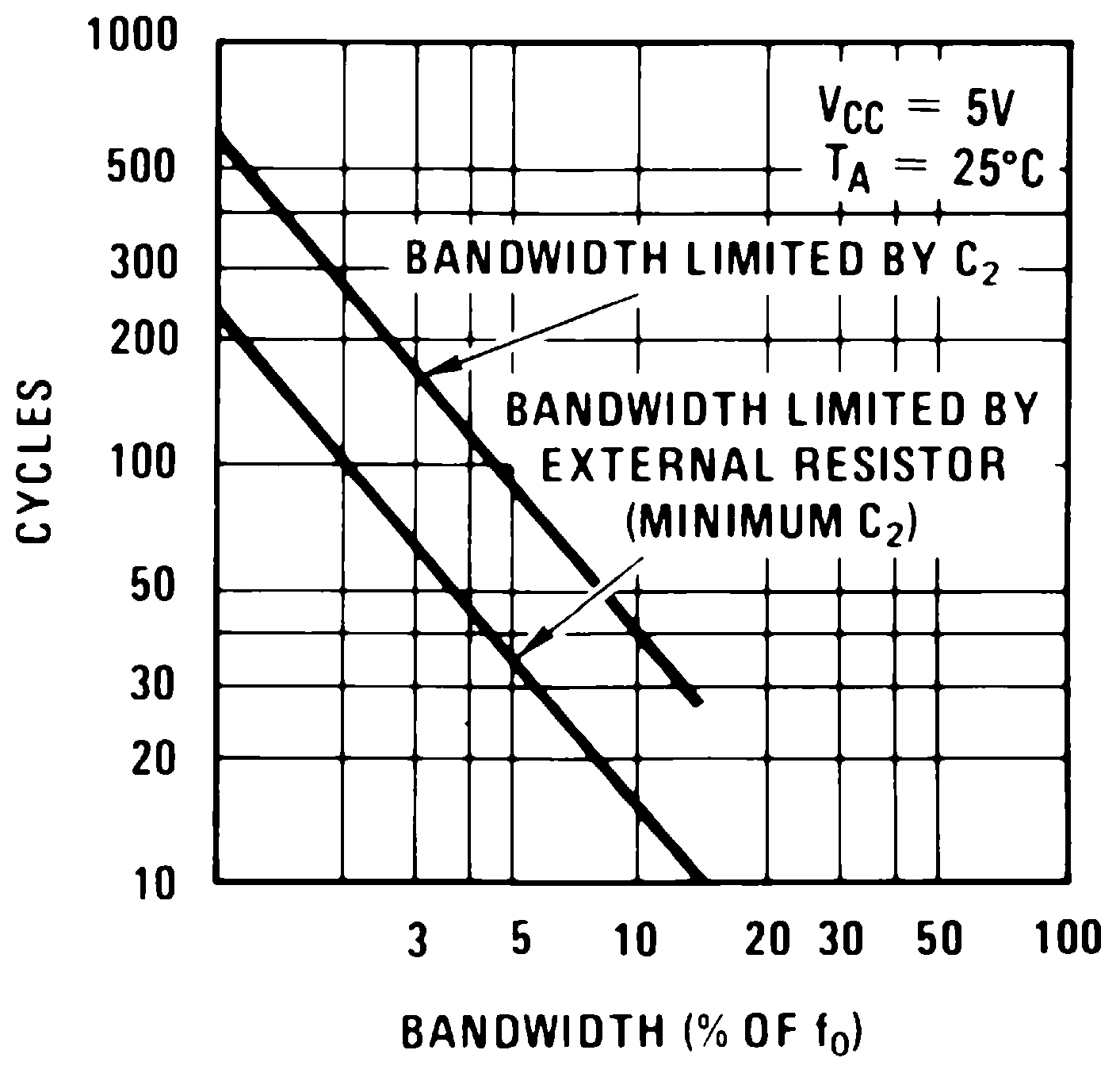
GUID-0497F205-F2E8-457F-9486-F5F1058C9C74-low.pngFigure 7-9 Greatest Number of Cycles Before Output
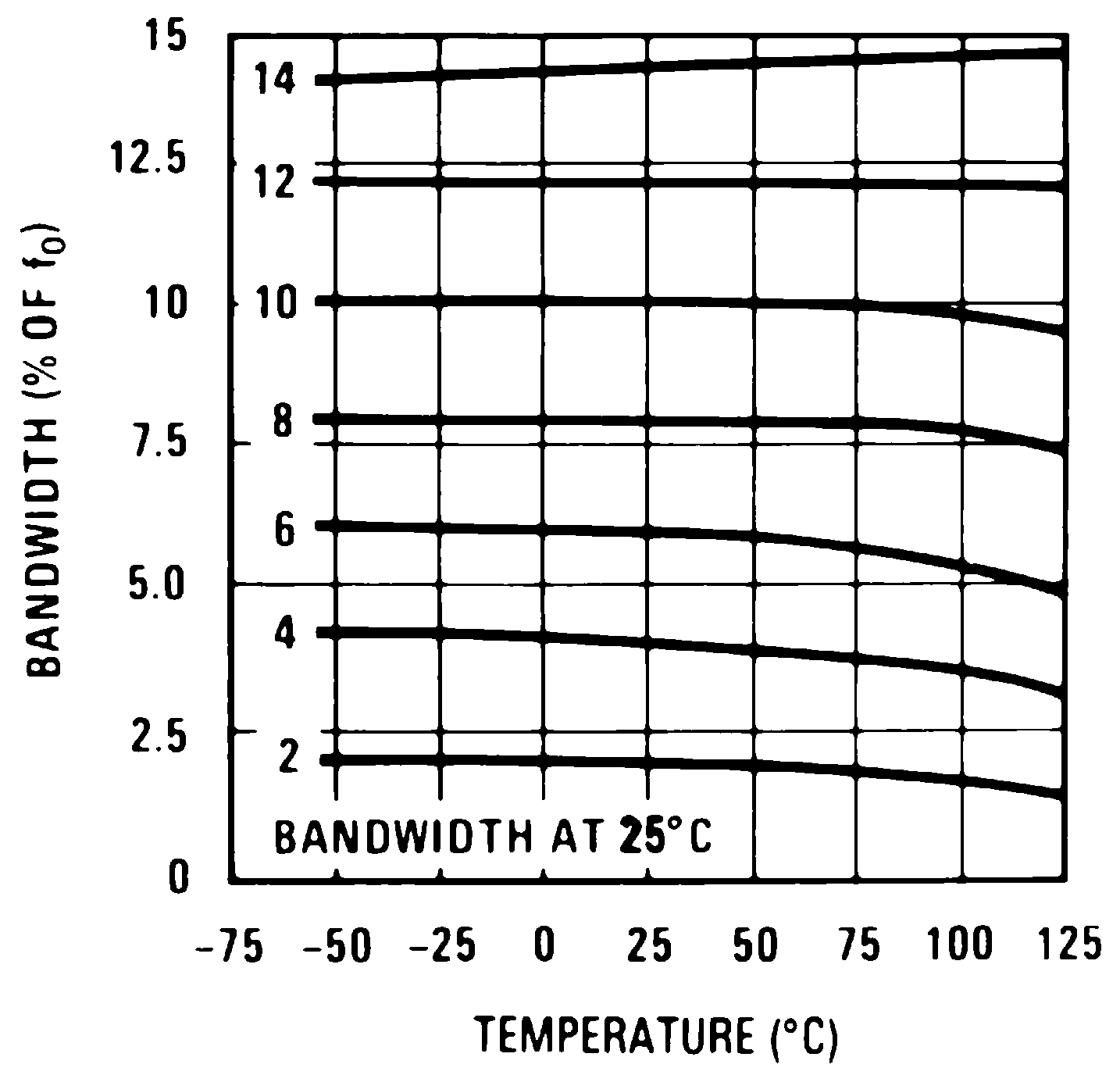
GUID-0180D8B8-3931-4953-A6B8-D116AD7D7CF2-low.pngFigure 7-2 Typical Bandwidth Variation
GUID-6F16FE61-C19B-47EC-B0A6-EAABA021AD64-low.pngFigure 7-4 Typical Frequency Drift
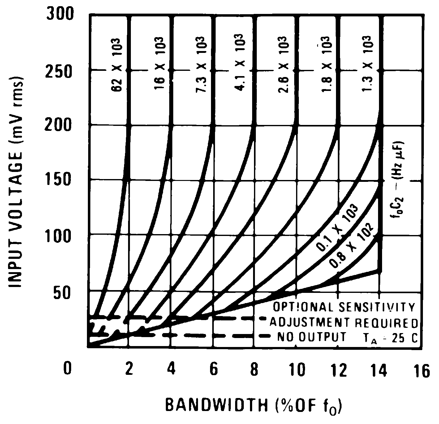
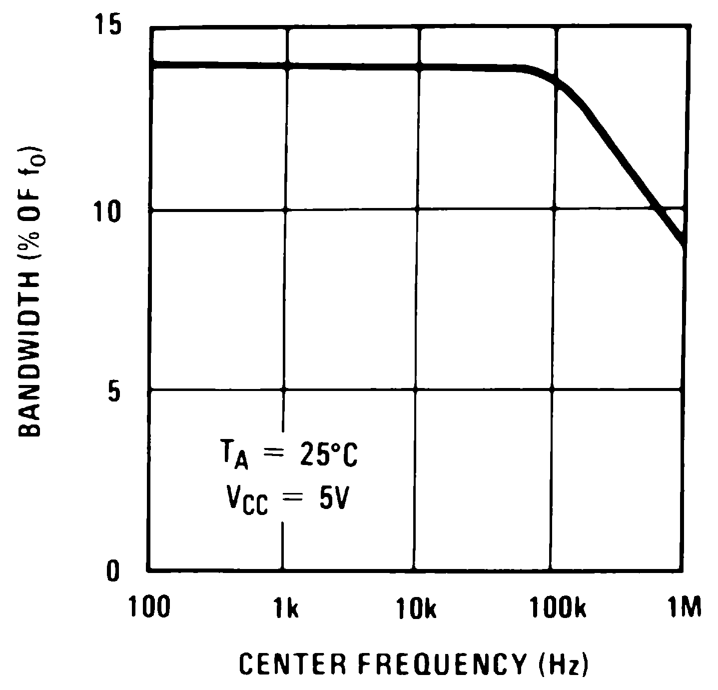
GUID-4BDC118F-A90F-4D71-B9C1-F1C89FCA4D83-low.pngFigure 7-6 Largest Detection Bandwidth
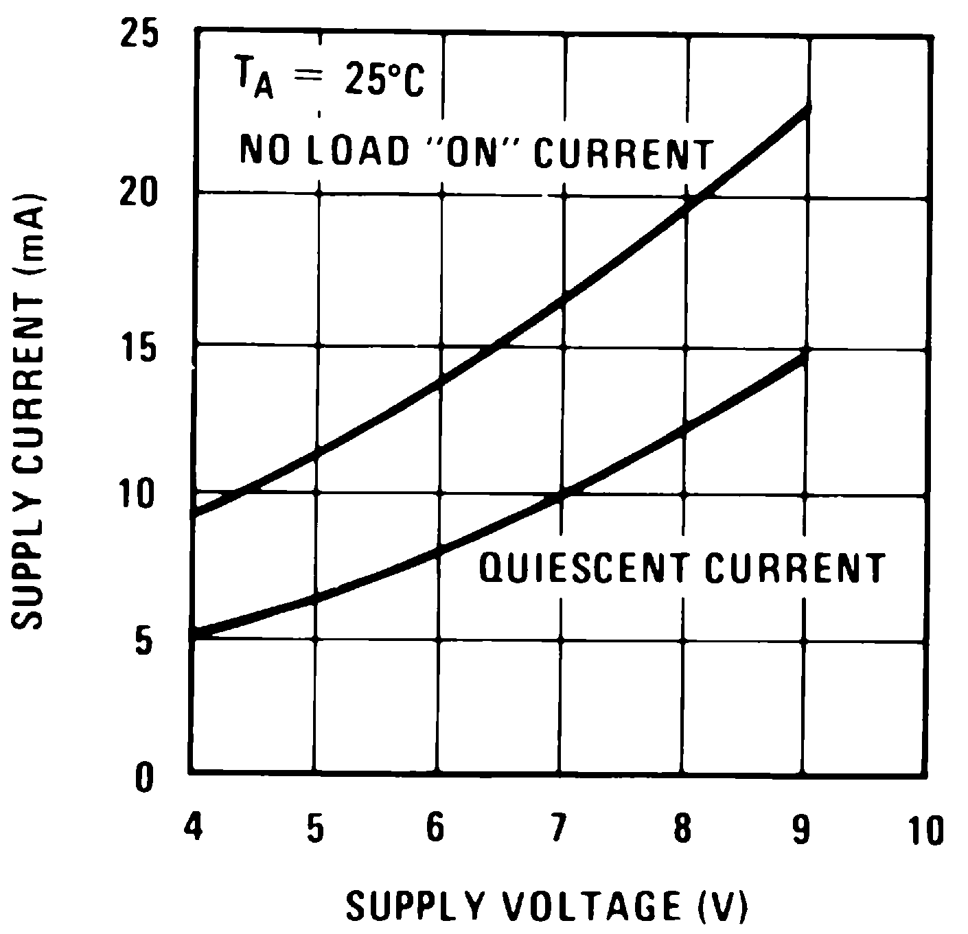
GUID-7BE51BCA-A5EE-4FD2-8AFD-175F7A08F0A0-low.pngFigure 7-8 Typical Supply Current vs Supply Voltage
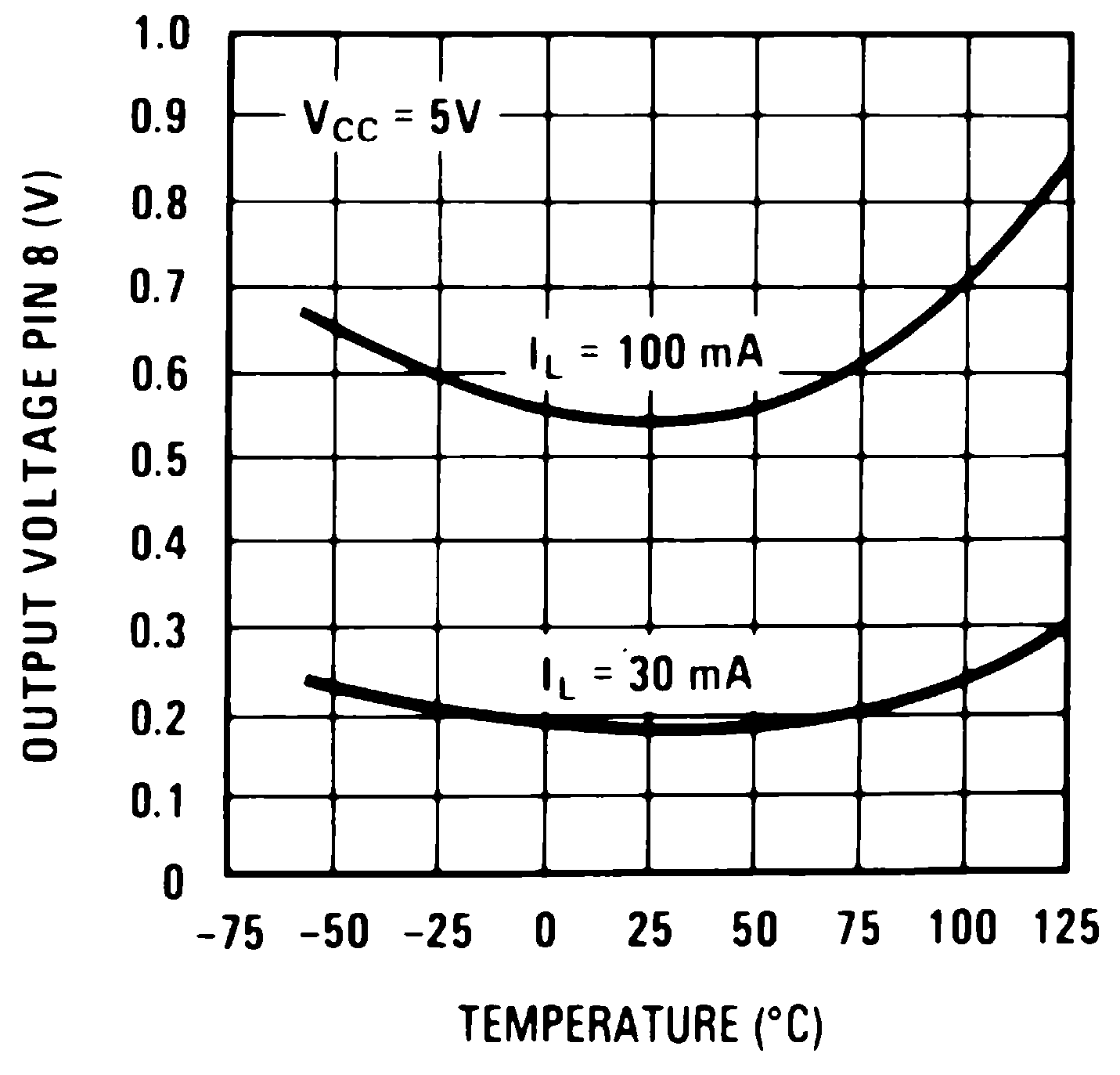
GUID-9D828EAB-63B9-4936-867D-FF5BD77153E2-low.pngFigure 7-10 Typical Output Voltage vs Temperature