SNOSBQ4F May   1999  – January 2022 LM567C

PRODUCTION DATA  

  1. Features
  2. Applications
  3. Description
  4. Revision History
  5. Device Comparison
  6. Pin Configuration and Functions
  7. Specifications
    1. 7.1 Absolute Maximum Ratings
    2. 7.2 Recommended Operating Conditions
    3. 7.3 Thermal Information
    4. 7.4 Electrical Characteristics
    5. 7.5 Typical Characteristics
  8. Parameter Measurement Information
  9. Detailed Description
    1. 9.1 Overview
    2. 9.2 Functional Block Diagram
    3. 9.3 Feature Description
      1. 9.3.1 Center Frequency
      2. 9.3.2 Output Filter
      3. 9.3.3 Loop Filter
      4. 9.3.4 Logic Output
      5. 9.3.5 Die Characteristics
    4. 9.4 Device Functional Modes
      1. 9.4.1 Operation With Vi < 200m – VRMS
      2. 9.4.2 Operation With Vi > 200m – VRMS
  10. 10Application and Implementation
    1. 10.1 Application Information
    2. 10.2 Typical Applications
      1. 10.2.1 Touch-Tone Decoder
        1. 10.2.1.1 Design Requirements
        2. 10.2.1.2 Detailed Design Procedure
          1. 10.2.1.2.1 Timing Components
          2. 10.2.1.2.2 Bandwidth
          3. 10.2.1.2.3 Output Filter
        3. 10.2.1.3 Application Curve
      2. 10.2.2 Oscillator with Quadrature Output
        1. 10.2.2.1 Design Requirements
        2. 10.2.2.2 Detailed Design Procedure
        3. 10.2.2.3 Application Curve
      3. 10.2.3 Oscillator with Double Frequency Output
        1. 10.2.3.1 Design Requirements
        2. 10.2.3.2 Detailed Design Procedure
        3. 10.2.3.3 Application Curve
      4. 10.2.4 Precision Oscillator Drive 100-mA Loads
        1. 10.2.4.1 Design Requirements
        2. 10.2.4.2 Detailed Design Procedure
        3. 10.2.4.3 Application Curve
      5. 10.2.5 AC Test Circuit
        1. 10.2.5.1 Design Requirements
        2. 10.2.5.2 Detailed Design Procedure
        3. 10.2.5.3 Application Curve
  11. 11Power Supply Recommendations
  12. 12Layout
    1. 12.1 Layout Guidelines
    2. 12.2 Layout Example
  13. 13Device and Documentation Support
    1. 13.1 Receiving Notification of Documentation Updates
    2. 13.2 Support Resources
    3. 13.3 Trademarks
    4. 13.4 Electrostatic Discharge Caution
    5. 13.5 Glossary
  14. 14Mechanical, Packaging, and Orderable Information

Package Options

Mechanical Data (Package|Pins)
Thermal pad, mechanical data (Package|Pins)
Orderable Information

Description

The LM567 and LM567C are general purpose tone decoders designed to provide a saturated transistor switch to ground when an input signal is present within the passband. The circuit consists of an I and Q detector driven by a voltage controlled oscillator which determines the center frequency of the decoder. External components are used to independently set center frequency, bandwidth and output delay.

Device Information(1)
PART NUMBERPACKAGEBODY SIZE (NOM)
LM567CSOIC (8)4.90 mm × 3.91 mm
PDIP (8)9.81 mm × 6.35 mm
For all available packages, see the orderable addendum at the end of the datasheet.
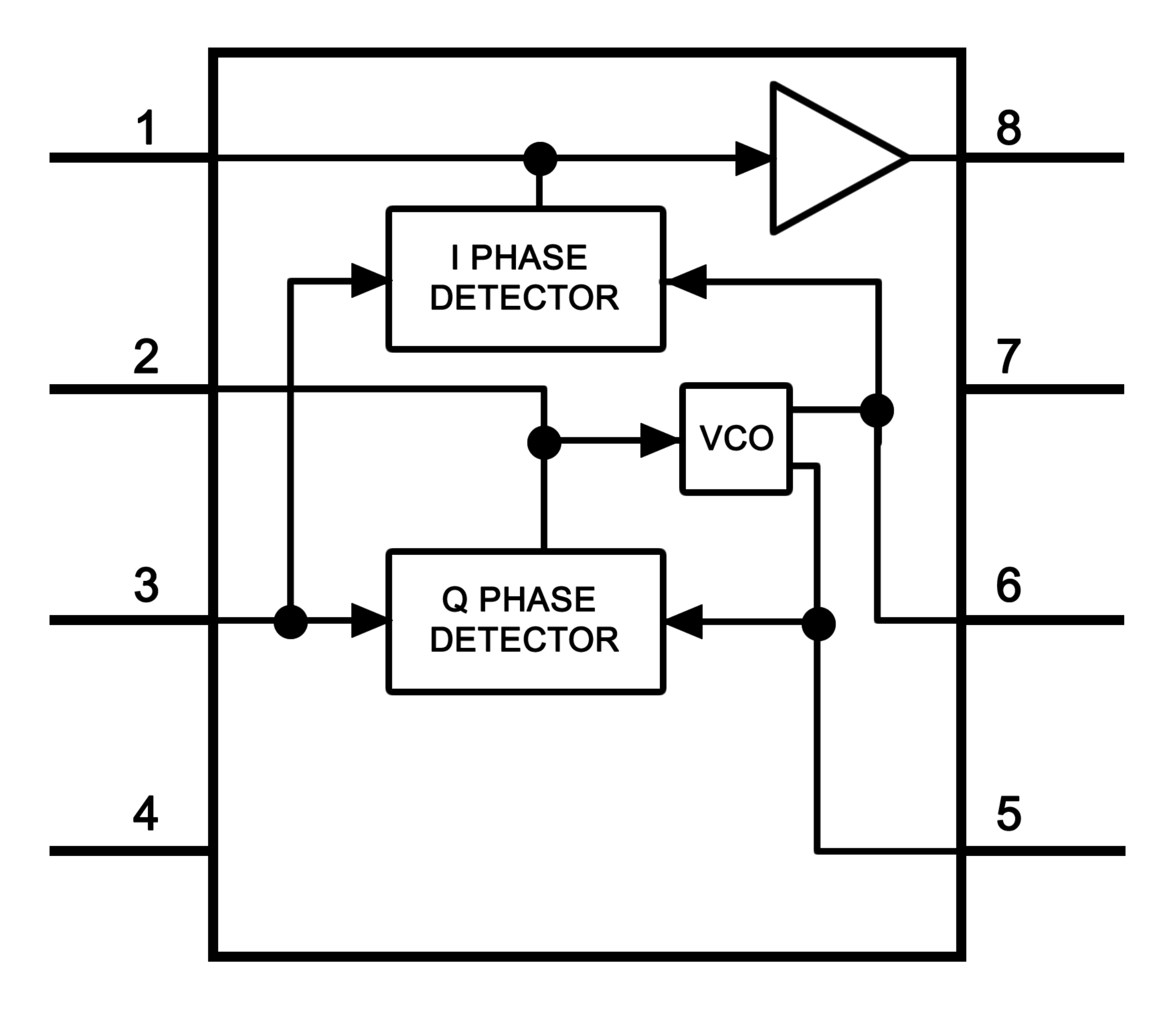
GUID-CB953B48-1375-4078-ACEE-31245DF07F4B-low.gif Simplified Diagram