SNOSC25D May 1998 – October 2015 LM741
PRODUCTION DATA.
- 1 Features
- 2 Applications
- 3 Description
- 4 Revision History
- 5 Pin Configuration and Functions
- 6 Specifications
- 7 Detailed Description
- 8 Application and Implementation
- 9 Power Supply Recommendations
- 10Layout
- 11Device and Documentation Support
- 12Mechanical, Packaging, and Orderable Information
Package Options
Mechanical Data (Package|Pins)
- YS|0
- P|8
Thermal pad, mechanical data (Package|Pins)
Orderable Information
7 Detailed Description
7.1 Overview
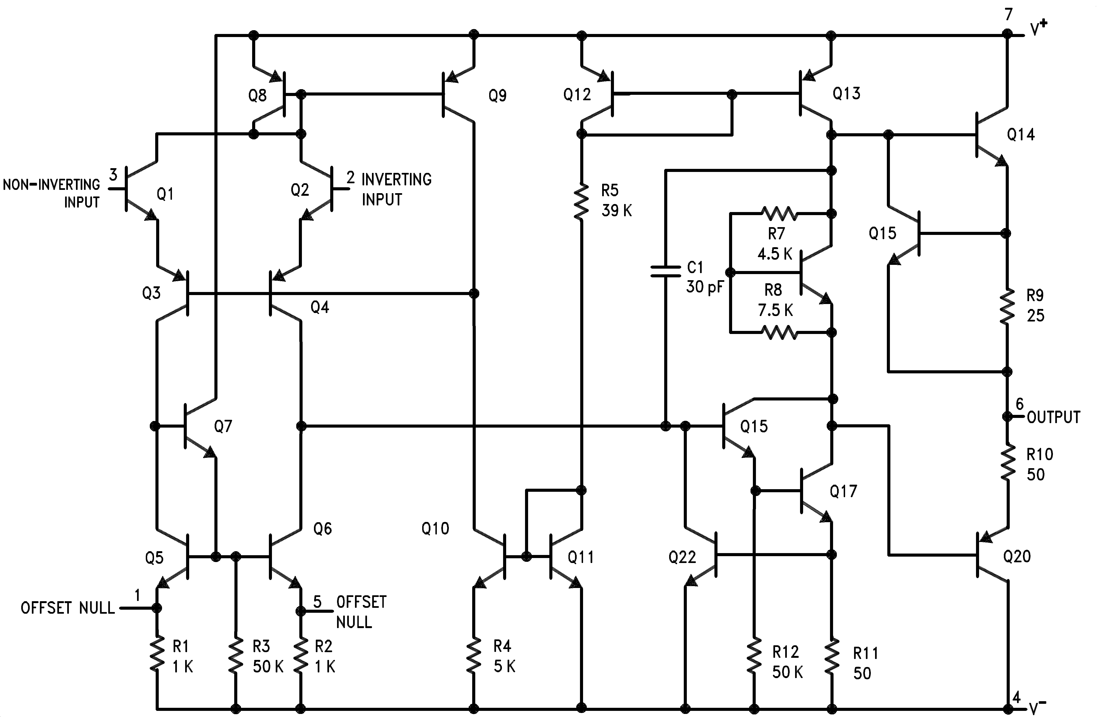
The LM74 devices are general-purpose operational amplifiers which feature improved performance over industry standards like the LM709. It is intended for a wide range of analog applications. The high gain and wide range of operating voltage provide superior performance in integrator, summing amplifier, and general feedback applications. The LM741 can operate with a single or dual power supply voltage. The LM741 devices are direct, plug-in replacements for the 709C, LM201, MC1439, and 748 in most applications.
7.2 Functional Block Diagram

7.3 Feature Description
7.3.1 Overload Protection
The LM741 features overload protection circuitry on the input and output. This prevents possible circuit damage to the device.
7.3.2 Latch-up Prevention
The LM741 is designed so that there is no latch-up occurrence when the common-mode range is exceeded. This allows the device to function properly without having to power cycle the device.
7.3.3 Pin-to-Pin Capability
The LM741 is pin-to-pin direct replacements for the LM709C, LM201, MC1439, and LM748 in most applications. Direct replacement capabilities allows flexibility in design for replacing obsolete parts.
7.4 Device Functional Modes
7.4.1 Open-Loop Amplifier
The LM741 can be operated in an open-loop configuration. The magnitude of the open-loop gain is typically large thus for a small difference between the noninverting and inverting input terminals, the amplifier output will be driven near the supply voltage. Without negative feedback, the LM741 can act as a comparator. If the inverting input is held at 0 V, and the input voltage applied to the noninverting input is positive, the output will be positive. If the input voltage applied to the noninverting input is negative, the output will be negative.
7.4.2 Closed-Loop Amplifier
In a closed-loop configuration, negative feedback is used by applying a portion of the output voltage to the inverting input. Unlike the open-loop configuration, closed loop feedback reduces the gain of the circuit. The overall gain and response of the circuit is determined by the feedback network rather than the operational amplifier characteristics. The response of the operational amplifier circuit is characterized by the transfer function.