SNOSC25D May   1998  – October 2015 LM741

PRODUCTION DATA.  

  1. Features
  2. Applications
  3. Description
  4. Revision History
  5. Pin Configuration and Functions
  6. Specifications
    1. 6.1 Absolute Maximum Ratings
    2. 6.2 ESD Ratings
    3. 6.3 Recommended Operating Conditions
    4. 6.4 Thermal Information
    5. 6.5 Electrical Characteristics, LM741
    6. 6.6 Electrical Characteristics, LM741A
    7. 6.7 Electrical Characteristics, LM741C
  7. Detailed Description
    1. 7.1 Overview
    2. 7.2 Functional Block Diagram
    3. 7.3 Feature Description
      1. 7.3.1 Overload Protection
      2. 7.3.2 Latch-up Prevention
      3. 7.3.3 Pin-to-Pin Capability
    4. 7.4 Device Functional Modes
      1. 7.4.1 Open-Loop Amplifier
      2. 7.4.2 Closed-Loop Amplifier
  8. Application and Implementation
    1. 8.1 Application Information
    2. 8.2 Typical Application
      1. 8.2.1 Design Requirements
      2. 8.2.2 Detailed Design Procedure
      3. 8.2.3 Application Curve
  9. Power Supply Recommendations
  10. 10Layout
    1. 10.1 Layout Guidelines
    2. 10.2 Layout Example
  11. 11Device and Documentation Support
    1. 11.1 Community Resources
    2. 11.2 Trademarks
    3. 11.3 Electrostatic Discharge Caution
    4. 11.4 Glossary
  12. 12Mechanical, Packaging, and Orderable Information

Package Options

Mechanical Data (Package|Pins)
Thermal pad, mechanical data (Package|Pins)
Orderable Information

5 Pin Configuration and Functions

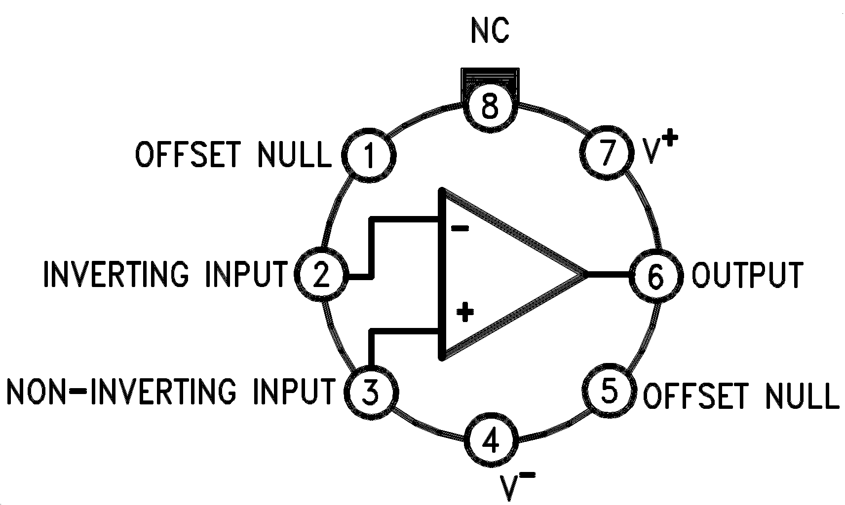
LMC Package
8-Pin TO-99
Top View
LM741 00934102.png
LM741H is available per JM38510/10101
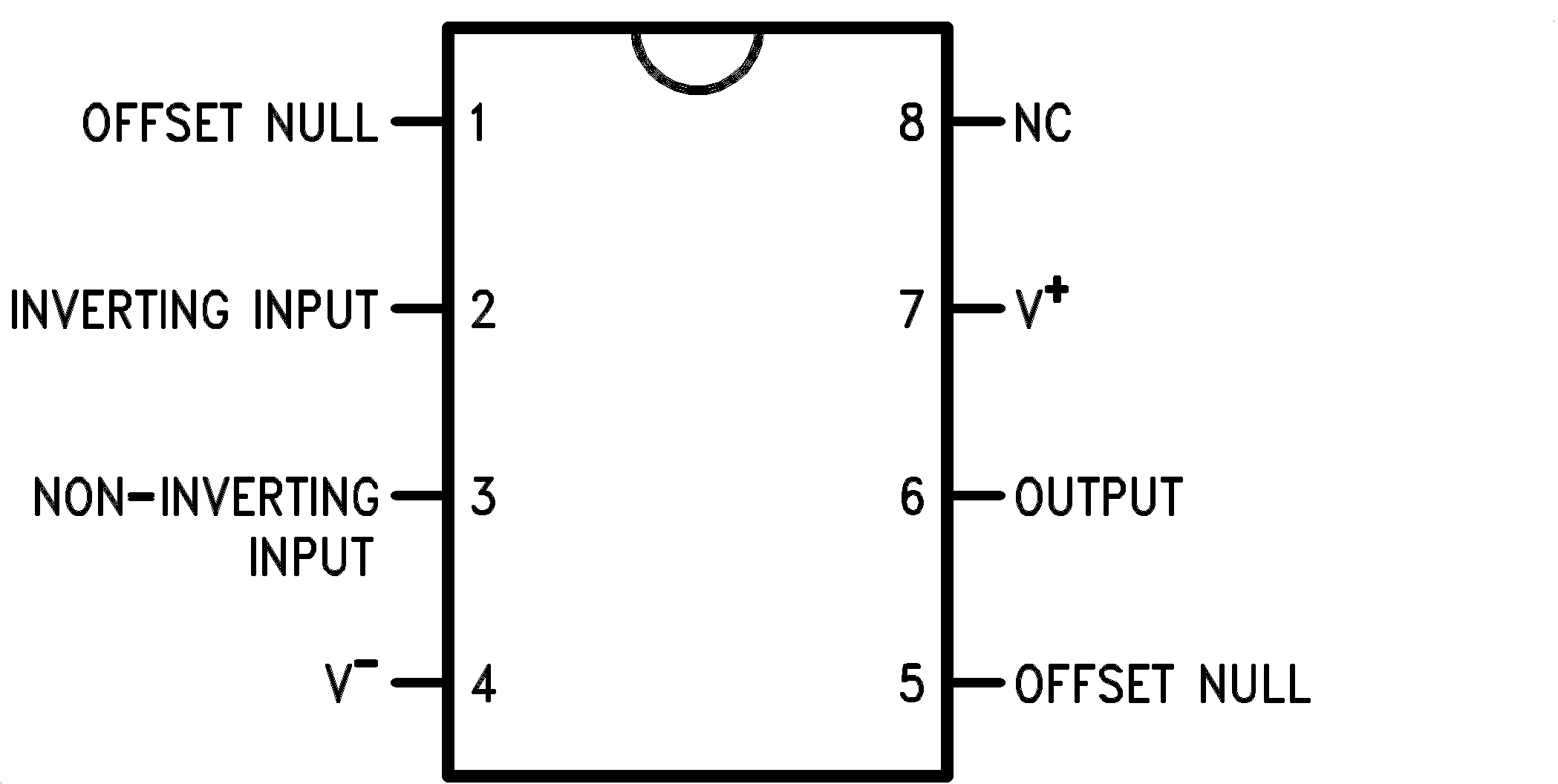
NAB Package
8-Pin CDIP or PDIP
Top View
LM741 00934103.png

Pin Functions

PIN I/O DESCRIPTION
NAME NO.
INVERTING INPUT 2 I Inverting signal input
NC 8 N/A No Connect, should be left floating
NONINVERTING INPUT 3 I Noninverting signal input
OFFSET NULL 1, 5 I Offset null pin used to eliminate the offset voltage and balance the input voltages.
OFFSET NULL
OUTPUT 6 O Amplified signal output
V+ 7 I Positive supply voltage
V– 4 I Negative supply voltage