SNIS139F February 2005 – January 2024 LM95231
PRODUCTION DATA
- 1
- 1 Features
- 2 Applications
- 3 Description
- 4 Pin Configuration and Functions
- 5 Specifications
- 6 Detailed Description
-
7 Registers
- 7.1 LM95231 Registers
- 7.2 Status Register
- 7.3 Configuration Register
- 7.4 Remote Diode Filter Control Register
- 7.5 Remote Diode Model Type Select Register
- 7.6 Remote TruTherm Mode Control
- 7.7 Local and Remote MSB and LSB Temperature Registers
- 7.8 Manufacturers ID Register
- 7.9 Die Revision Code Register
- 8 Application and Implementation
- 9 Layout
- 10Device and Documentation Support
- 11Revision History
- 12Mechanical, Packaging, and Orderable Information
Package Options
Mechanical Data (Package|Pins)
- DGK|8
Thermal pad, mechanical data (Package|Pins)
Orderable Information
5.5 Logic Electrical Characteristics SMBus Digital Switching Characteristics
Unless otherwise noted, these specifications apply for VDD=+3.0 Vdc
to +3.6 Vdc, CL (load capacitance) on output lines = 80 pF.
Boldface limits apply for TA = TJ = TMIN
to TMAX; all other limits TA = TJ =
+25°C, unless otherwise noted.
The switching characteristics of the LM95231 fully meet or exceed the published specifications of the SMBus version 2.0. The following parameters are the timing relationships between SMBCLK and SMBDAT signals related to the LM95231. They adhere to but are not necessarily the SMBus bus specifications.
The switching characteristics of the LM95231 fully meet or exceed the published specifications of the SMBus version 2.0. The following parameters are the timing relationships between SMBCLK and SMBDAT signals related to the LM95231. They adhere to but are not necessarily the SMBus bus specifications.
| Symbol | Parameter | Conditions | Typical(1) | Limits(4) | Units (Limit) |
|---|---|---|---|---|---|
| fSMB | SMBus Clock Frequency | 100 10 |
kHz (max) kHz (min) |
||
| tLOW | SMBus Clock Low Time | from VIN(0)max to VIN(0)max | 4.7 25 |
µs (min) ms (max) |
|
| tHIGH | SMBus Clock High Time | from VIN(1)min to VIN(1)min | 4.0 | µs (min) | |
| tR,SMB | SMBus Rise Time | See(3) | 1 | µs (max) | |
| tF,SMB | SMBus Fall Time | See(4) | 0.3 | µs (max) | |
| tOF | Output Fall Time | CL = 400pF, IO = 3mA(4) |
250 | ns (max) | |
| tTIMEOUT | SMBDAT and SMBCLK Time Low for Reset of Serial Interface(5) | 25 35 |
ms (min) ms (max) |
||
| tSU;DAT | Data In Setup Time to SMBCLK High | 250 | ns (min) | ||
| tHD;DAT | Data Out Stable after SMBCLK Low | 300 1075 |
ns (min) ns (max) |
||
| tHD;STA | Start Condition SMBDAT Low to SMBCLK Low (Start condition hold before the first clock falling edge) | 100 | ns (min) | ||
| tSU;STO | Stop Condition SMBCLK High to SMBDAT Low (Stop Condition Setup) | 100 | ns (min) | ||
| tSU;STA | SMBus Repeated Start-Condition Setup Time, SMBCLK High to SMBDAT Low | 0.6 | µs (min) | ||
| tBUF | SMBus Free Time Between Stop and Start Conditions | 1.3 | µs (min) |
(1) Absolute Maximum Ratings indicate limits beyond which damage to
the device may occur. Operating Ratings indicate conditions for which the device
is ensured to be functional, but do not ensure specific performance limits. For
ensured specifications and test conditions, see the Electrical Characteristics.
The ensured specifications apply only for the test condition listed. Some
performance characteristics may degrade when the device is not operated under
the listed test conditions. Operation of the device beyond the Maximum Operating
Ratings is not recommended.
(2) When the input voltage (VI) at any pin exceeds the
power supplies (VI < GND or VI > VDD),
the current at that pin should be limited to 5 mA. Parasitic components and or
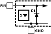
ESD protection circuitry are shown in Figure 5-1 and Table 5-1 for the LM95231's pins. Care should be taken not to forward bias the
parasitic diode, D1, present on pins: D1+, D2+, D1−, D2−. Doing so by more than
50 mV may corrupt the temperature measurements.
(4) Human body model, 100pF discharged through a 1.5kΩ resistor.
Machine model, 200pF discharged directly into each pin.
(5) Reflow temperature profiles are different for packages
containing lead (Pb) than for those that do not.
(1) Typicals are at TA = 25°C and represent most likely
parametric norm at time of product characterization. The typical specifications
are not ensured.
(4) Limits are specified to AOQL (Average Outgoing Quality
Level).
(3) Local temperature accuracy does not include the effects of
self-heating. The rise in temperature due to self-heating is the product of the
internal power dissipation of the LM95231 and the thermal resistance. See Note 2 of the Operating Ratings table for the thermal resistance to
be used in the self-heating calculation.
(5) The accuracy of the LM95231 is ensured when using the thermal
diode of Pentium 4 processor on 90nm process or an MMBT3904 type transistor, as
selected in the Remote Diode Model Select register.
(7) Quiescent current will not increase substantially when the
SMBus is active.
(6) This specification is provided only to indicate how often
temperature data is updated. The LM95231 can be read at any time without regard
to conversion state (and will yield last conversion result).
(3) The output rise time is measured from (VIN(0)max +
0.15V) to (VIN(1)min − 0.15V).
(4) The output fall time is measured from (VIN(1)min -
0.15V) to (VIN(1)min + 0.15V).
(5) Holding the SMBDAT and/or SMBCLK lines Low for a time interval
greater than tTIMEOUT will reset the LM95231's SMBus state machine,
therefore setting SMBDAT and SMBCLK pins to a high impedance state.
 Figure 5-1 SMBus
Communication
Figure 5-1 SMBus
CommunicationTable 5-1 Parasitic components and ESD
protection circuitry
| Pin # | Circuit | Pin ESD Protection Structure Circuits | |
|---|---|---|---|
| 1 | A | 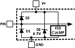 |
 |
| 2 | A | ||
| 3 | A | ||
| 4 | A | Circuit A | Circuit C |
| 5 | B | 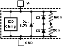 |
|
| 6 | B | Circuit B | |
| 7 | C | ||
| 8 | C | ||