SNLS530D April 2016 – June 2018 LMH1219
PRODUCTION DATA.
- 1 Features
- 2 Applications
- 3 Description
- 4 Revision History
- 5 Pin Configuration and Functions
- 6 Specifications
-
7 Detailed Description
- 7.1 Overview
- 7.2 Functional Block Diagram
- 7.3
Feature Description
- 7.3.1 4-Level Input Configuration Pins
- 7.3.2 Input Carrier Detect
- 7.3.3 -6 dB Splitter Mode Launch Amplitude for IN0
- 7.3.4 Continuous Time Linear Equalizer (CTLE)
- 7.3.5 Input-Output Mux Selection
- 7.3.6 Clock and Data Recovery (CDR) Reclocker
- 7.3.7 Internal Eye Opening Monitor (EOM)
- 7.3.8 Output Function Control
- 7.3.9 Output Driver Amplitude and De-Emphasis Control
- 7.3.10 Status Indicators and Interrupts
- 7.3.11 Additional Programmability
- 7.4 Device Functional Modes
- 7.5 LMH1219 Register Map
- 8 Application and Implementation
- 9 Power Supply Recommendations
- 10Layout
- 11Device and Documentation Support
- 12Mechanical, Packaging, and Orderable Information
Package Options
Mechanical Data (Package|Pins)
- RTW|24
Thermal pad, mechanical data (Package|Pins)
- RTW|24
Orderable Information
3 Description
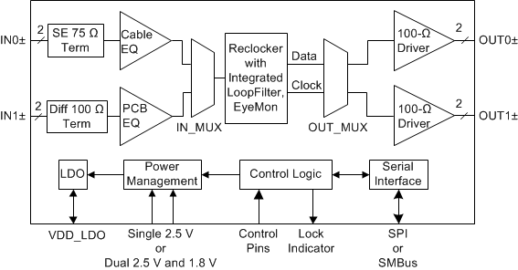
The LMH1219 is a low-power, dual-input and dual-output, adaptive equalizer with integrated reclocker. It supports SMPTE video rates up to 11.88 Gbps and 10 GbE video over IP, enabling UHD video for 4K/8K applications. An extended reach adaptive cable equalizer at IN0 is designed to equalize data transmitted over 75 Ω coaxial cable and operates over a wide range of data rates from 125 Mbps to 11.88 Gbps. An adaptive board trace equalizer at IN1 is SFF-8431 compatible and supports both SMPTE and 10 GbE data rates.
The integrated reclocker attenuates high frequency jitter and provides the best signal integrity. High input jitter tolerance of the reclocker improves timing margin. The reclocker has a built-in loop filter, and operates without the need of a precision input reference clock. A non-disruptive eye monitor allows real time measurement of the serial data to simplify system debug and accelerate board bring-up.
The integrated 2:1 Mux and 1:2 Fanout provide flexibility for multiple video signals. The output drivers offer programmable de-emphasis to compensate board trace losses at its outputs. The integrated return loss network meets stringent SMPTE specifications across all data rates. The typical power consumption of LMH1219 is 250 mW. In the absence of input signal, power is further reduced to 16 mW.
The LMH1219 is pin compatible to LMH1226 (12G UHD reclocker) and LMH0324 (3G adaptive cable equalizer).
Device Information(1)
| PART NUMBER | PACKAGE | BODY SIZE (NOM) |
|---|---|---|
| LMH1219 | QFN (24) | 4.00 mm × 4.00 mm |
- For all available packages, see the orderable addendum at the end of the data sheet.
Simplified Block Diagram
