SNLS530D April   2016  – June 2018 LMH1219

PRODUCTION DATA.  

  1. Features
  2. Applications
  3. Description
    1.     Simplified Block Diagram
  4. Revision History
  5. Pin Configuration and Functions
    1.     Pin Functions
  6. Specifications
    1. 6.1 Absolute Maximum Ratings
    2. 6.2 ESD Ratings
    3. 6.3 Recommended Operating Conditions
    4. 6.4 Thermal Information
    5. 6.5 Electrical Characteristics
    6. 6.6 Recommended SMBus Interface AC Timing Specifications
    7. 6.7 Serial Parallel Interface (SPI) AC Timing Specifications
    8. 6.8 Typical Characteristics
  7. Detailed Description
    1. 7.1 Overview
    2. 7.2 Functional Block Diagram
    3. 7.3 Feature Description
      1. 7.3.1  4-Level Input Configuration Pins
      2. 7.3.2  Input Carrier Detect
      3. 7.3.3  -6 dB Splitter Mode Launch Amplitude for IN0
      4. 7.3.4  Continuous Time Linear Equalizer (CTLE)
        1. 7.3.4.1 Adaptive Cable Equalizer (IN0+)
        2. 7.3.4.2 Adaptive PCB Trace Equalizer (IN1±)
      5. 7.3.5  Input-Output Mux Selection
      6. 7.3.6  Clock and Data Recovery (CDR) Reclocker
      7. 7.3.7  Internal Eye Opening Monitor (EOM)
      8. 7.3.8  Output Function Control
      9. 7.3.9  Output Driver Amplitude and De-Emphasis Control
      10. 7.3.10 Status Indicators and Interrupts
        1. 7.3.10.1 LOCK_N (Lock Indicator)
        2. 7.3.10.2 CD_N (Carrier Detect)
        3. 7.3.10.3 INT_N (Interrupt)
      11. 7.3.11 Additional Programmability
        1. 7.3.11.1 Cable Length Indicator (CLI)
        2. 7.3.11.2 Digital MUTEREF
    4. 7.4 Device Functional Modes
      1. 7.4.1 System Management Bus (SMBus) Mode
        1. 7.4.1.1 SMBus Read and Write Transactions
          1. 7.4.1.1.1 SMBus Write Operation Format
          2. 7.4.1.1.2 SMBus Read Operation Format
      2. 7.4.2 Serial Peripheral Interface (SPI) Mode
        1. 7.4.2.1 SPI Read and Write Transactions
          1. 7.4.2.1.1 SPI Write Transaction Format
          2. 7.4.2.1.2 SPI Read Transaction Format
        2. 7.4.2.2 SPI Daisy Chain
    5. 7.5 LMH1219 Register Map
      1. 7.5.1 Share Register Page
      2. 7.5.2 CTLE/CDR Register Page
      3. 7.5.3 CableEQ/Drivers Register Page
  8. Application and Implementation
    1. 8.1 Application Information
      1. 8.1.1 General Guidance for SMPTE and 10 GbE Applications
      2. 8.1.2 Optimizing Time to Adapt and Lock
      3. 8.1.3 LMH1219 and LMH0324 Compatibility
    2. 8.2 Typical Application
      1. 8.2.1 Design Requirements
      2. 8.2.2 Detail Design Procedure
      3. 8.2.3 Recommended VOD and DEM Register Settings
      4. 8.2.4 Application Performance Plots
  9. Power Supply Recommendations
  10. 10Layout
    1. 10.1 PCB Layout Guidelines
    2. 10.2 Layout Example
  11. 11Device and Documentation Support
    1. 11.1 Receiving Notification of Documentation Updates
    2. 11.2 Community Resources
    3. 11.3 Trademarks
    4. 11.4 Electrostatic Discharge Caution
    5. 11.5 Glossary
  12. 12Mechanical, Packaging, and Orderable Information

Package Options

Mechanical Data (Package|Pins)
Thermal pad, mechanical data (Package|Pins)
Orderable Information

Typical Application

The LMH1219 is a low-power cable equalizer with integrated reclocker that supports SDI data rates up to 11.88 Gbps and 10 GbE. Figure 22 shows a typical implementation of the LMH1219 as a SDI adaptive cable equalizer at IN0+. Signal attenuated by a long coax cable is applied to the LMH1219 at the BNC port. Signal from a 10 GbE optical module is connected to the input port at IN1±. Equalized and reclocked data is output at OUT0± and OUT1± to a downstream video processor.
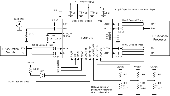
LMH1219 spi_mode_connection_diagram_snls475.gifFigure 22. LMH1219 SPI Mode Connection Diagram