SNOSAT7G August 2007 – October 2015 LMP7300
PRODUCTION DATA.
- 1 Features
- 2 Applications
- 3 Description
- 4 Revision History
- 5 Pin Configuration and Functions
- 6 Specifications
- 7 Detailed Description
- 8 Application and Implementation
- 9 Power Supply Recommendations
- 10Layout
- 11Device and Documentation Support
- 12Mechanical, Packaging, and Orderable Information
Package Options
Mechanical Data (Package|Pins)
Thermal pad, mechanical data (Package|Pins)
Orderable Information
7 Detailed Description
7.1 Overview
The LMP7300 device is a unique combination of micropower and precision. The open collector comparator has low offset, high CMRR, high PSRR, programmable hysteresis and microamp supply current. The precision 2.048-V reference provides a DAC or ADC with an accurate binary divisible voltage. The comparator and reference combination forms an ideal single IC solution for low power sensor or portable applications.
7.2 Functional Block Diagram
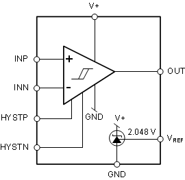
7.3 Feature Description
7.3.1 Voltage Reference
The reference output voltage is a band gap derived 2.048 V that is trimmed to achieve typically 0.2% accuracy over the full operating temperature range of −40°C to 125°C. The trim procedure employs a curvature correction algorithm to compensate for the base emitter thermal nonlinearity inherent in band gap design topologies. The reference accuracy and the set resistor tolerance determine the magnitude and precision of the programmable hysteresis. In situations where reference noise filtering is required, TI recommends a 5-µF capacitor in series with a 190-Ω resistor to ground.
7.3.2 Comparator
7.3.2.1 Output Stage
The comparator employs an open collector output stage that can switch microamp loads for micropower precision threshold detection to applications requiring activating a solenoid, a lamp, or an LED. The wired-OR type output easily interfaces to TTL, CMOS, or multiple outputs, as in a window comparator application, over a range of 0.5 V to 12 V. The output is capable of driving greater than 10-mA output current and yet maintaining a saturation voltage less than 0.4 V over temperature. The supply current increases linearly when driving heavy loads, so TI recommends a pullup resistor of 100 kΩ or greater for micropower applications.
7.3.2.2 Fault Detection Rate
The user’s choice of a pullup resistor and capacitive load determines the minimum response time and the event detection rate. By optimizing overdrive, the pullup resistor and capactive load fault update rates of 200 kHz to 250 kHz or greater can be achieved.
7.3.3 Hysteresis
False triggering on noise coupled into the signal path is a common problem for comparator based threshold detectors. One of the most effective solutions is to add hysteresis. Hysteresis is a circuit signal path characteristic where an amplitude delay is introduced to the normal input. Positive hysteresis forces the signal to pass the normal switch point before the output makes a low to high transition while negative hysteresis does the opposite. This is a memory effect. The comparator behaves differently based on which direction the signal is going.
The LM7300 has been designed with a unique way of introducing hysteresis. The set points are completely independent of each other, the power supply, and the input or output conditions. The HYSTP pin sets positive hysteresis and the HYSTN pin sets the negative hysteresis in a simple way using two resistors. The pins can be tied together for the same hysteresis or tied to separate voltage taps for asymmetric hysteresis, or tied to the reference for no hysteresis. When the precision reference is used to drive the voltage tap resistor divider precise, stable threshold levels can be obtained. The maximum recommended hysteresis is about 130 mV. This places the HYSTP and HYSTN pin voltages at VREF – 130 mV, which is approximately the center of their input common mode range at 2.7 V. For the typical example, a differential input signal voltage, VIN, is applied between INP and INN, the noninverting and inverting inputs of the comparator. A DC switch or threshold voltage, VTH, is set on the negative input to keep the output off when the signal is above and on when it goes below this level. For a precision threshold tie the INN pin to VREF. With the output, off the circuit is in the minimum power state. Figure 13 through Figure 21 demonstrate the different configurations for setting the upper threshold VIH and the lower threshold VIL and their relationship to the input trip point VREF, by the following formulas.
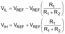
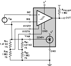 Figure 12. Typical Micropower Application to Set Asymmetric Positive and
Negative Hysteresis of −10 mV, 3 mV
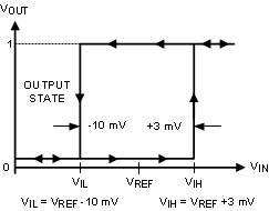 Figure 13. Typical Micropower Application to Set Asymmetric Positive and
Negative Hysteresis of −10 mV, 3 mV
When VID = 0, INN = INP = VTH
Figure 15 shows the configuration with no hysteresis when the HYSTP and HYSTN pins are connected together to VREF. TI does not recommend this configuration because it has the highest level of false triggers due to the system noise.
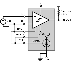 Figure 14. Typical Configuration for No Hysteresis
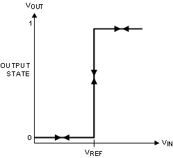 Figure 15. Typical Configuration for No Hysteresis
Figure 17 shows the configuration with symmetric hysteresis when the HYSTP and HYSTN pins are connected to the same voltage that is less than VREF. The two trip points set a hysteresis band around the input threshold voltage VREF, such that the positive band is equal to the negative band.
This configuration controls the false triggering mentioned in Figure 15. For precise level detection applications, TI recommends symmetric hysteresis values less than 5 mV to 10 mV.
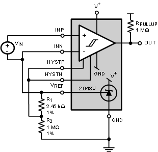 Figure 16. Symmetric Hysteresis ±5 mV
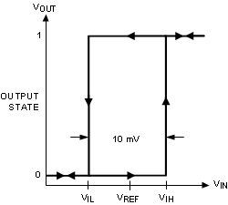 Figure 17. Symmetric Hysteresis ±5 mV
Figure 19 shows the case for negative hysteresis by biasing only the HYSN pin to a voltage less than VREF.
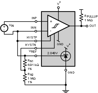 Figure 18. Typical Configuration for Negative Hysteresis = −10 mV
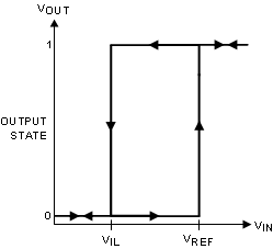 Figure 19. Typical Configuration for Negative Hysteresis = −10 mV
The case for setting only a positive hysteresis is demonstrated in Figure 21.
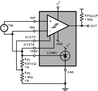 Figure 20. Connections for Positive Hysteresis = 10 mV
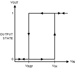 Figure 21. Connections for Positive Hysteresis = 10 mV
In the general case, as demonstrated with both positive and negative hysteresis bands in Figure 22, noise within these bands has no effect on the state of the comparator output. In Example 1 the noise is well behaved and in band. The output is clean and well behaved. In Example 2, a significant amount of out of band noise is present; however, due to hysteresis no false triggers occur on the rising positive or falling negative edges. The hysteresis forces the signal level to move higher or lower before the output is set to the opposite state.
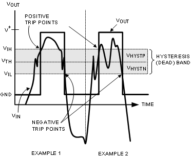 Figure 22. Output Response With Input Noise Less than Hysteresis Band
7.3.3.1 How Much Hysteresis Is Correct?
An effective way of determining the minimum hysteresis necessary for clean switching is to decrease the amount of hysteresis until false triggering is observed, and then use a multiple of say three times that amount of hysteresis in the final circuit. This is most easily accomplished in the breadboard phase by making R1 and R2 potentiometers. For applications near or above 100°C, TI recommends a minimum of 5-mV hysteresis due to peaking of the LMP7300 noise sensitivity at high temperatures.
7.4 Device Functional Modes
The LMP7300 device may be used as a voltage reference or as a comparator with HIGH and LOW output states. A LOW output will occur when the noninverting input (INP) is less than the inverting input (INN). A HIGH output will occur when the noninverting input (INP) is greater than the inverting input (INN).