SNOSAT7G August 2007 – October 2015 LMP7300
PRODUCTION DATA.
- 1 Features
- 2 Applications
- 3 Description
- 4 Revision History
- 5 Pin Configuration and Functions
- 6 Specifications
- 7 Detailed Description
- 8 Application and Implementation
- 9 Power Supply Recommendations
- 10Layout
- 11Device and Documentation Support
- 12Mechanical, Packaging, and Orderable Information
Package Options
Mechanical Data (Package|Pins)
Thermal pad, mechanical data (Package|Pins)
Orderable Information
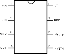
5 Pin Configuration and Functions
DGK or D Package
8-Pin VSSOP or SOIC
Top View

Pin Functions
| PIN | TYPE(1) | DESCRIPTION | |
|---|---|---|---|
| NAME | NO. | ||
| +IN | 1 | I | Noninverting Comparator Input. The +IN has a common-mode voltage range from 1 V above the negative rail to, and including, the positive rail. Internal ESD diodes, connected from the +IN pin to the rails, protect the input stage from overvoltage. If the input voltage exceeds the rails, the diodes turn on and clamp the input to a safe level. |
| -IN | 2 | I | Inverting Comparator Input. The −IN has a common-mode voltage range from 1 V above the negative rail to, and including, the positive rail. Internal ESD diodes, connected from the −IN pin to the rails, protects the input stage from overvoltage. If the input voltage exceeds the rails, the diodes turn on and clamp the input to a safe level. |
| GND | 3 | G | Ground. This pin may be connected to a negative DC voltage source for applications requiring a dual supply. If connected to a negative supply, decouple this pin with 0.1-µF ceramic capacitor to ground. The internal reference output voltage is referenced to this pin. GND is the die substrate connection. |
| OUT | 4 | O | Comparator Output. The output is an open-collector. It can drive voltage loads by using a pullup resistor, or it can drive current loads by sinking a maximum output current. This pin may be taken to a maximum of +12 V with respect to the ground pin, irrespective of supply voltage. |
| HYSTN | 5 | I | Negative Hysteresis pin. This pin sets the lower trip voltage VIL. The common mode range is from 1V above the negative rail to VCC. The input signal must fall below VIL for the comparator to switch from high to low state. |
| HYSTP | 6 | I | Positive Hysteresis pin. This pin sets the upper trip voltage VIH. The common mode range is from 1V above the negative rail to VCC. The input signal must rise above VIH for the comparator to switch from low to high state. |
| REF | 7 | O | Reference Voltage Output pin. This is the output pin of a 2.048-V band gap precision reference. |
| V+ | 8 | P | Positive Supply Terminal. The supply voltage range is 2.7 V to 12 V. Decouple this pin with 0.1-μF ceramic capacitor to ground. |
(1) P= Power, G=Ground, I=Input, O=Output, A=Analog