SNVS852D June   2012  – August 2018 LMZ20502

PRODUCTION DATA.  

  1. Features
  2. Applications
  3. Description
    1.     Device Images
      1.      Simplified Schematic
      2.      Typical Efficiency for VOUT = 1.8 V Auto Mode
  4. Revision History
  5. Pin Configuration and Functions
    1.     Pin Functions
  6. Specifications
    1. 6.1 Absolute Maximum Ratings
    2. 6.2 ESD Ratings
    3. 6.3 Recommended Operating Conditions
    4. 6.4 Thermal Information
    5. 6.5 Electrical Characteristics
    6. 6.6 System Characteristics
    7. 6.7 Typical Characteristics
  7. Detailed Description
    1. 7.1 Overview
    2. 7.2 Functional Block Diagram
    3. 7.3 Feature Description
      1. 7.3.1 Nano Scale Package
      2. 7.3.2 Internal Synchronous Rectifier
      3. 7.3.3 Current Limit Protection
      4. 7.3.4 Start-Up
      5. 7.3.5 Dropout Behavior
      6. 7.3.6 Power Good Flag Function
      7. 7.3.7 Thermal Shutdown
    4. 7.4 Device Functional Modes
      1. 7.4.1 PWM Operation
      2. 7.4.2 PFM Operation
  8. Application and Implementation
    1. 8.1 Application Information
    2. 8.2 Typical Application
      1. 8.2.1 Detailed Design Procedure
        1. 8.2.1.1 Custom Design With WEBENCH® Tools
        2. 8.2.1.2 Setting The Output Voltage
        3. 8.2.1.3 Output and Feed-Forward Capacitors
        4. 8.2.1.4 Input Capacitors
        5. 8.2.1.5 Maximum Ambient Temperature
        6. 8.2.1.6 Options
      2. 8.2.2 Application Curves
    3. 8.3 Do's and Don'ts
  9. Power Supply Recommendations
  10. 10Layout
    1. 10.1 Layout Guidelines
    2. 10.2 Layout Example
    3. 10.3 Soldering Information
  11. 11Device and Documentation Support
    1. 11.1 Device Support
      1. 11.1.1 Third-Party Products Disclaimer
      2. 11.1.2 Development Support
        1. 11.1.2.1 Custom Design With WEBENCH® Tools
      3. 11.1.3 Documentation Support
        1. 11.1.3.1 Related Documentation
    2. 11.2 Receiving Notification of Documentation Updates
    3. 11.3 Community Resources
    4. 11.4 Trademarks
    5. 11.5 Electrostatic Discharge Caution
    6. 11.6 Glossary
  12. 12Mechanical, Packaging, and Orderable Information
    1. 12.1 Tape and Reel Information

Package Options

Refer to the PDF data sheet for device specific package drawings

Mechanical Data (Package|Pins)
  • SIL|8
Thermal pad, mechanical data (Package|Pins)
Orderable Information

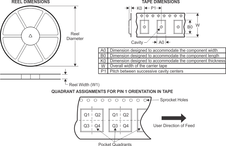
Tape and Reel Information

LMZ20502 Tape_and_Reel_Dims.gif
Device Package
Type
Package Drawing Pins SPQ Reel
Diameter (mm)
Reel
Width W1 (mm)
A0
(mm)
B0
(mm)
K0
(mm)
P1
(mm)
W
(mm)
Pin1
Quadrant
LMZ20502SILR uSiP SIL 8 3000 330.0 12.4 3.75 3.75 2.2 8.0 12.0 Q2
LMZ20502SILT uSiP SIL 8 250 178.0 13.2 3.75 3.75 2.2 8.0 12.0 Q2

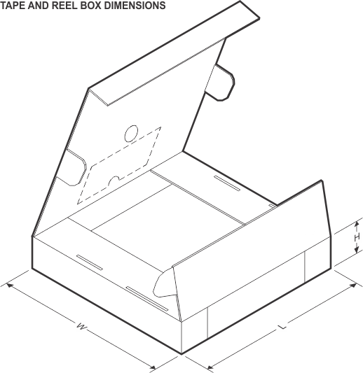
LMZ20502 Tape_and_Reel_Box_Dims.gif

Device Package Type Package Drawing Pins SPQ Length (mm) Width (mm) Height (mm)
LMZ20502SILR uSiP SIL 8 3000 383.0 353.0 58.0
LMZ20502SILT uSiP SIL 8 250 223.0 194.0 35.0