SDLS967H may 2016 – july 2023 LSF0108-Q1
PRODMIX
- 1
- 1 Features
- 2 Applications
- 3 Description
- 4 Revision History
- 5 Pin Configuration and Functions
-
6 Specifications
- 6.1 Absolute Maximum Ratings
- 6.2 ESD Ratings
- 6.3 Recommended Operating Conditions
- 6.4 Thermal Information (Q1)
- 6.5 Electrical Characteristics - RKS Package
- 6.6 Electrical Characteristics - PW Package
- 6.7 Switching Characteristics (Translating Down)
- 6.8 Switching Characteristics (Translating Up)
- 6.9 Typical Characteristics
- 7 Parameter Measurement Information
- 8 Detailed Description
- 9 Applications and Implementation
- 10Device and Documentation Support
- 11Mechanical, Packaging, and Orderable Information
Package Options
Mechanical Data (Package|Pins)
Thermal pad, mechanical data (Package|Pins)
Orderable Information
9.2.1.2.3 LSF0108-Q1 Bandwidth
The maximum frequency of the LSF0108-Q1 is dependent on the application. The device can operate at speeds of >100 MHz given the correct conditions. The maximum frequency is dependent upon the loading of the application. The LSF0108-Q1 behaves like a standard switch where the bandwidth of the device is dictated by the on resistance and on capacitance of the device.
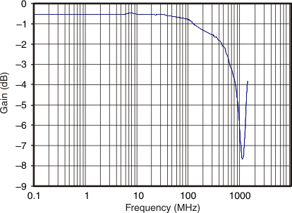
Figure 9-3 shows a bandwidth measurement of the LSF0108-Q1 using a two-port network analyzer.
 Figure 9-3 3-dB Bandwidth
The 3-dB point of the LSF0108-Q1 is ≅ 600 MHz; however, this measurement is an analog type of measurement. For digital applications the signal should not degrade up to the fifth harmonic of the digital signal. The frequency bandwidth should be at least five times the maximum digital clock rate. This component of the signal is very important in determining the overall shape of the digital signal. In the case of the LSF0108-Q1, a digital clock frequency of greater than 100 MHz can be achieved.
The LSF0108-Q1 does not provide any drive capability. Therefore higher frequency applications will require higher drive strength from the host side. No pull-up resistor is needed on the host side (3.3 V) if the LSF0108-Q1 is being driven by standard CMOS totem pole output driver. Ideally, it is best to minimize the trace length from the LSF0108-Q1 on the sink side (1.8 V) to minimize signal degradation.
All fast edges have an infinite spectrum of frequency components; however, there is an inflection (or knee) in the frequency spectrum of fast edges where frequency components higher than ƒknee are insignificant in determining the shape of the signal.
To calculate the maximum practical frequency component, or the knee frequency (fknee), use Equation 4 and Equation 5:
For signals with rise time characteristics based on 10% to 90% thresholds, fknee is equal to 0.5 divided by the rise time of the signal. For signals with rise time characteristics based on 20% to 80% thresholds, which is very common in many of today's device specifications, ƒknee is equal to 0.4 divided by the rise time of the signal.
Some guidelines to follow that will help maximize the performance of the device:
- Keep trace length to a minimum by placing the LSF0108-Q1 close to the I2C output of the processor.
- The trace length should be less than half the time of flight to reduce ringing and line reflections or non-monotonic behavior in the switching region.
- To reduce overshoots, a pull-up resistor can be added on the 1.8 V side; be aware that a slower fall time is to be expected.