SCPS146G October   2005  – March 2021 PCA9544A

PRODUCTION DATA  

  1. Features
  2. Applications
  3. Description
  4. Revision History
  5. Pin Configuration and Functions
  6. Specifications
    1. 6.1 Absolute Maximum Ratings
    2. 6.2 ESD Ratings
    3. 6.3 Recommended Operating Conditions
    4. 6.4 Thermal Information
    5. 6.5 Electrical Characteristics
    6. 6.6 I2C Interface Timing Requirements
    7. 6.7 Switching Characteristics
    8. 6.8 Interrupt Timing Requirements
  7. Parameter Measurement Information
  8. Detailed Description
    1. 8.1 Overview
    2. 8.2 Functional Block Diagram
    3. 8.3 Feature Description
    4. 8.4 Device Functional Modes
      1. 8.4.1 Power-On Reset
    5. 8.5 Programming
      1. 8.5.1 I2C Interface
    6. 8.6 Register Map
      1. 8.6.1 Control Register
        1. 8.6.1.1 Device Address
        2. 8.6.1.2 Control Register Description
        3. 8.6.1.3 Control Register Definition
        4. 8.6.1.4 Interrupt Handling
  9. Application Information Disclaimer
    1. 9.1 Application Information
    2. 9.2 Typical Application
      1. 9.2.1 Design Requirements
      2. 9.2.2 Detailed Design Procedure
      3. 9.2.3 Application Curves
  10. 10Power Supply Recommendations
    1. 10.1 Power-On Reset Requirements
  11. 11Layout
    1. 11.1 Layout Guidelines
    2. 11.2 Layout Example
  12. 12Device and Documentation Support
    1. 12.1 Receiving Notification of Documentation Updates
    2. 12.2 Support Resources
    3. 12.3 Trademarks
    4. 12.4 Electrostatic Discharge Caution
    5. 12.5 Glossary
  13. 13Mechanical, Packaging, and Orderable Information

Package Options

Mechanical Data (Package|Pins)
Thermal pad, mechanical data (Package|Pins)
Orderable Information

Device Address

Following a start condition, the bus master must output the address of the slave it is accessing. The address of the PCA9544A is shown in Figure 8-7. To conserve power, no internal pull-up resistors are incorporated on the hardware-selectable address pins, and they must be pulled high or low.
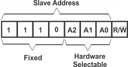
GUID-4D3E0544-26D4-4FF6-8502-29F3698422A2-low.gifFigure 8-7 PCA9544A Address

The last bit of the slave address defines the operation to be performed. When set to a logic 1, a read is selected, while a logic 0 selects a write operation.