SLDS216 December 2017 PGA302
PRODUCTION DATA.
- 1 Features
- 2 Applications
- 3 Description
- 4 Revision History
- 5 Description (continued)
- 6 Pin Configuration and Functions
-
7 Specifications
- 7.1 Absolute Maximum Ratings
- 7.2 ESD Ratings
- 7.3 Recommended Operating Conditions
- 7.4 Thermal Information
- 7.5 Overvoltage and Reverse Voltage Protection
- 7.6 Linear Regulators
- 7.7 Internal Reference
- 7.8 Internal Oscillator
- 7.9 Bridge Sensor Supply
- 7.10 Temperature Sensor Supply
- 7.11 Bridge Offset Cancel
- 7.12 P Gain and T Gain Input Amplifiers (Chopper Stabilized)
- 7.13 Analog-to-Digital Converter
- 7.14 Internal Temperature Sensor
- 7.15 Bridge Current Measurement
- 7.16 One Wire Interface
- 7.17 DAC Output
- 7.18 DAC Gain for DAC Output
- 7.19 Non-Volatile Memory
- 7.20 Diagnostics - PGA30x
- 7.21 Typical Characteristics
-
8 Detailed Description
- 8.1 Overview
- 8.2 Functional Block Diagram
- 8.3
Feature Description
- 8.3.1 Overvoltage and Reverse Voltage Protection
- 8.3.2 Linear Regulators
- 8.3.3 Internal Reference
- 8.3.4 Internal Oscillator
- 8.3.5 VBRGP and VBRGN Supply for Resistive Bridge
- 8.3.6 ITEMP Supply for Temperature Sensor
- 8.3.7 P Gain
- 8.3.8 T Gain
- 8.3.9 Bridge Offset Cancel
- 8.3.10 Analog-to-Digital Converter
- 8.3.11 Internal Temperature Sensor
- 8.3.12 Bridge Current Measurement
- 8.3.13 Digital Interface
- 8.3.14 OWI
- 8.3.15 I2C Interface
- 8.3.16 DAC Output
- 8.3.17 DAC Gain for DAC Output
- 8.3.18 Memory
- 8.3.19 Diagnostics
- 8.3.20 Digital Compensation and Filter
- 8.3.21 Revision ID
- 8.4 Device Functional Modes
- 8.5
Register Maps
- 8.5.1
Programmer's Model
- 8.5.1.1 Memory Map
- 8.5.1.2
Control and Status Registers
- 8.5.1.2.1 MICRO_INTERFACE_CONTROL (DI Page Address = 0x0) (DI Page Offset = 0x0C)
- 8.5.1.2.2 PSMON1 (M0 Address= 0x40000558) (DI Page Address = 0x2) (DI Page Offset = 0x58)
- 8.5.1.2.3 AFEDIAG (M0 Address= 0x4000055A) (DI Page Address = 0x2) (DI Page Offset = 0x5A)
- 8.5.1.2.4 P_GAIN_SELECT (DI Page Address = 0x2) (DI Page Offset = 0x47)
- 8.5.1.2.5 T_GAIN_SELECT (DI Page Address = 0x2) (DI Page Offset = 0x48)
- 8.5.1.2.6 TEMP_CTRL (DI Page Address = 0x2) (DI Page Offset = 0x4C)
- 8.5.1.2.7 OFFSET_CANCEL (DI Page Address = 0x2) (DI Page Offset = 0x4E)
- 8.5.1.2.8 PADC_DATA1 (DI Page Address = 0x0) (DI Page Offset = 0x10)
- 8.5.1.2.9 PADC_DATA2 (DI Page Address = 0x0) (DI Page Offset = 0x11)
- 8.5.1.2.10 TADC_DATA1 (DI Page Address = 0x0) (DI Page Offset = 0x14)
- 8.5.1.2.11 TADC_DATA2 (DI Page Address = 0x0) (DI Page Offset = 0x15)
- 8.5.1.2.12 DAC_REG0_1 (DI Page Address = 0x2) (DI Page Offset = 0x30)
- 8.5.1.2.13 DAC_REG0_2 (DI Page Address = 0x2) (DI Page Offset = 0x31)
- 8.5.1.2.14 OP_STAGE_CTRL (DI Page Address = 0x2) (DI Page Offset = 0x3B)
- 8.5.1.2.15 EEPROM_ARRAY (DI Page Address = 0x5) (DI Page Offset = 0x00 - 0x7F)
- 8.5.1.2.16 EEPROM_CACHE_BYTE0 (DI Page Address = 0x5) (DI Page Offset = 0x80)
- 8.5.1.2.17 EEPROM_CACHE_BYTE1 (DI Page Address = 0x5) (DI Page Offset = 0x81)
- 8.5.1.2.18 EEPROM_PAGE_ADDRESS (DI Page Address = 0x5) (DI Page Offset = 0x82)
- 8.5.1.2.19 EEPROM_CTRL (DI Page Address = 0x5) (DI Page Offset = 0x83)
- 8.5.1.2.20 EEPROM_CRC (DI Page Address = 0x5) (DI Page Offset = 0x84)
- 8.5.1.2.21 EEPROM_STATUS (DI Page Address = 0x5) (DI Page Offset = 0x85)
- 8.5.1.2.22 EEPROM_CRC_STATUS (DI Page Address = 0x5) (DI Page Offset = 0x86)
- 8.5.1.2.23 EEPROM_CRC_VALUE (DI Page Address = 0x5) (DI Page Offset = 0x87)
- 8.5.1.2.24 H0 (EEPROM Address= 0x40000000)
- 8.5.1.2.25 H1 (EEPROM Address= 0x40000002)
- 8.5.1.2.26 H2 (EEPROM Address= 0x40000004)
- 8.5.1.2.27 H3 (EEPROM Address= 0x40000006)
- 8.5.1.2.28 G0 (EEPROM Address= 0x40000008)
- 8.5.1.2.29 G1 (EEPROM Address= 0x4000000A)
- 8.5.1.2.30 G2 (EEPROM Address= 0x4000000C)
- 8.5.1.2.31 G3 (EEPROM Address= 0x4000000E)
- 8.5.1.2.32 N0 (EEPROM Address= 0x40000010)
- 8.5.1.2.33 N1 (EEPROM Address= 0x40000012)
- 8.5.1.2.34 N2 (EEPROM Address= 0x40000014)
- 8.5.1.2.35 N3 (EEPROM Address= 0x40000016)
- 8.5.1.2.36 M0 (EEPROM Address= 0x40000018)
- 8.5.1.2.37 M1 (EEPROM Address= 0x4000001A)
- 8.5.1.2.38 M2 (EEPROM Address= 0x4000001C)
- 8.5.1.2.39 M3 (EEPROM Address= 0x4000001E)
- 8.5.1.2.40 PADC_GAIN (EEPROM Address= 0x40000020)
- 8.5.1.2.41 TADC_GAIN (EEPROM Address= 0x40000021)
- 8.5.1.2.42 PADC_OFFSET (EEPROM Address= 0x40000022)
- 8.5.1.2.43 TADC_OFFSET (EEPROM Address= 0x40000024)
- 8.5.1.2.44 TEMP_SW_CTRL (EEPROM Address= 0x40000028)
- 8.5.1.2.45 DAC_FAULT_MSB (EEPROM Address= 0x4000002A)
- 8.5.1.2.46 LPF_A0_MSB (EEPROM Address= 0x4000002B)
- 8.5.1.2.47 LPF_A1 (EEPROM Address= 0x4000002C)
- 8.5.1.2.48 LPF_A2 (EEPROM Address= 0x4000002E)
- 8.5.1.2.49 .LPF_B1 (EEPROM Address= 0x40000030)
- 8.5.1.2.50 NORMAL_LOW (EEPROM Address= 0x40000032)
- 8.5.1.2.51 NORMAL_HIGH (EEPROM Address= 0x40000034)
- 8.5.1.2.52 LOW_CLAMP (EEPROM Address= 0x40000036)
- 8.5.1.2.53 HIGH_CLAMP (EEPROM Address= 0x40000038)
- 8.5.1.2.54 DIAG_BIT_EN (EEPROM Address= 0x4000003A)
- 8.5.1
Programmer's Model
- 9 Application and Implementation
- 10Power Supply Recommendations
- 11Layout
- 12Device and Documentation Support
- 13Mechanical, Packaging, and Orderable Information
Package Options
Mechanical Data (Package|Pins)
- PW|16
Thermal pad, mechanical data (Package|Pins)
Orderable Information
7 Specifications
7.1 Absolute Maximum Ratings(1)
| MIN | MAX | UNIT | |||
|---|---|---|---|---|---|
| VDD | VDD voltage | –20 | 20 | V | |
| VOUT | VOUT voltage | –20 | 20 | V | |
| Voltage at VP_OTP | –0.3 | 8 | V | ||
| Voltage at sensor input and drive pins | –0.3 | 5 | V | ||
| Voltage at any IO pin | –0.3 | 2 | V | ||
| IDD, Short on VOUT | Supply current | 25 | mA | ||
| TJmax | Maximum junction temperature | 155 | °C | ||
| Tlead | Lead temperature (soldering, 10 s) | 260 | °C | ||
| Tstg | Storage temperature | –40 | 150 | °C | |
(1) Stresses beyond those listed under Absolute Maximum Ratings may cause permanent damage to the device. These are stress ratings only and functional operation of the device at these or any other conditions beyond those indicated under Recommended Operating Conditions are not implied. Exposure to Absolute-Maximum-Rated conditions for extended periods may affect device reliability.
7.2 ESD Ratings
| VALUE | UNIT | ||||
|---|---|---|---|---|---|
| V(ESD) | Electrostatic discharge | Human-body model (HBM), per ANSI/ESDA/JEDEC JS-001(1) | All pins except 9 and 10 | ±2000 | V |
| Pins 9 and 10 | ±4000 | ||||
| Charged-device model (CDM), per JEDEC specification JESD22-C101(2) | All pins except 1, 8, 9, and 16 | ±500 | |||
| Pins 1, 8, 9, and 16 | ±750 | ||||
(1) JEDEC document JEP155 states that 500-V HBM allows safe manufacturing with a standard ESD control process.
(2) JEDEC document JEP157 states that 250-V CDM allows safe manufacturing with a standard ESD control process.
7.3 Recommended Operating Conditions
over operating free-air temperature range (unless otherwise noted)| MIN | NOM | MAX | UNIT | |||
|---|---|---|---|---|---|---|
| VDD | Power supply voltage | 4.5 | 5 | 5.5(1) | V | |
| Slew Rate | VDD = 0 to 5 V; decoupling capacitor on VDD = 10 nF | 5 | V/ns | |||
| IDD | Power supply current - Normal Operation | No load on VBRG, No load on DAC | 6.5 | 10 | mA | |
| TA | Operating ambient temperature | –40 | 150 | °C | ||
| Programming temperature | EEPROM | –40 | 140 | °C | ||
| Start-up time (including analog and digital) | VDD ramp rate 1 V/µs | 250 | µs | |||
| Capacitor on VDD Pin | Not including series resistance | 100 | nF | |||
(1) The analog circuits in the device will be shut off for VDD>OVP. However, digital logic inside the device will continue to operate. The device will withstand VDD<VDD_ABSMAX without damage
7.4 Thermal Information
| THERMAL METRIC(1) | PGA302 | UNIT | |
|---|---|---|---|
| PW (TSSOP) | |||
| 16 PINS | |||
| RθJA | Junction-to-ambient thermal resistance | 96.8 | °C/W |
| RθJC(top) | Junction-to-case (top) thermal resistance | 27.3 | °C/W |
| RθJB | Junction-to-board thermal resistance | 43.3 | °C/W |
| ψJT | Junction-to-top characterization parameter | 1.2 | °C/W |
| ψJB | Junction-to-board characterization parameter | 42.7 | °C/W |
(1) For more information about traditional and new thermal metrics, see the IC Package Thermal Metrics application report.
7.5 Overvoltage and Reverse Voltage Protection
over operating free-air temperature range (unless otherwise noted)| PARAMETER | TEST CONDITIONS | MIN | TYP | MAX | UNIT | |
|---|---|---|---|---|---|---|
| Reverse voltage | –20 | V | ||||
| Overvoltage analog shutdown | –40°C to 150°C | 5.65 | V | |||
7.6 Linear Regulators
| PARAMETER | TEST CONDITIONS | MIN | TYP | MAX | UNIT | |
|---|---|---|---|---|---|---|
| VDVDD | DVDD voltage - operating | Capacitor on DVDD pin = 100 nF | 1.76 | 1.8 | 1.86 | V |
| VDVDD_POR | DVDD voltage - digital POR | 1.4 | 1.6 | 1.75 | V | |
| DVDD voltage - digital POR Hysteresis | 0.1 | V | ||||
| VVDD_POR | VDD voltage - digital POR | 4 | V | |||
| VDD voltage - digital POR Hysteresis | 0.1 | V | ||||
7.7 Internal Reference
over operating free-air temperature range (unless otherwise noted)| PARAMETER | TEST CONDITIONS | MIN | TYP | MAX | UNIT | |
|---|---|---|---|---|---|---|
| Reference voltage (including reference buffer) | 2.5 | V | ||||
| Reference initial error | –0.5% | 0.5% | ||||
| Reference voltage TC | –250 | 250 | ppm/°C | |||
| PSRR | VDD Ripple Conditions:
|
–35 | dB | |||
7.8 Internal Oscillator
| PARAMETER | TEST CONDITIONS | MIN | TYP | MAX | UNIT | |
|---|---|---|---|---|---|---|
| INTERNAL OSCILLATOR | ||||||
| Internal oscillator frequency | TA = 25°C | 8 | MHz | |||
| Internal oscillator frequency variation | Across operating temperature | –3% | 3% | |||
7.9 Bridge Sensor Supply
| PARAMETER | TEST CONDITIONS | MIN | TYP | MAX | UNIT | |
|---|---|---|---|---|---|---|
| VBRG SUPPLY FOR RESISTIVE BRIDGE SENSORS | ||||||
| VBRGP-VBRGN | Bridge supply voltage | ILOAD = 0 to 8.5mA | 2.4 | 2.5 | 2.6 | V |
| PMISMATCH | Mismatch between bridge supply voltage, temperature variation, and ADC reference temperature variation | Procedure to calculate drift mismatch:
|
–250 | +250 | ppm/°C | |
| IBRG | Current Supply to the Bridge | 8.5 | mA | |||
| Bridge short-circuit current limit | TA = 25°C; VVDD= 5 V |
9 | 25 | mA | ||
| CBRG | Capacitive Load | RBRG = 5 kΩ | 2 | nF | ||
7.10 Temperature Sensor Supply
| PARAMETER | TEST CONDITIONS | MIN | TYP | MAX | UNIT | |
|---|---|---|---|---|---|---|
| ITEMP SUPPLY FOR TEMPERATURE SENSOR(1) | ||||||
| ITEMP | Current supply to temperature sensor | Control bit = 0b000 | 45 | 50 | 55 | µA |
| Control bit = 0b001 | 90 | 100 | 110 | |||
| Control bit = 0b010 | 180 | 200 | 220 | |||
| Control bit = 0b011 | 850 | 1000 | 1150 | |||
| Control bit = 0b1xx | OFF | |||||
| TMISMATCH | Mismatch between ITEMP temperature variation and ADC reference temperature variation | Procedure to calculate drift mismatch:
|
–250 | +250 | ppm/°C | |
| ZOUT | Output Impedance | Ensured by design | 15 | MΩ | ||
| CTEMP | Capacitive load | 100 | nF | |||
(1) Not applicable for 8-pin package options
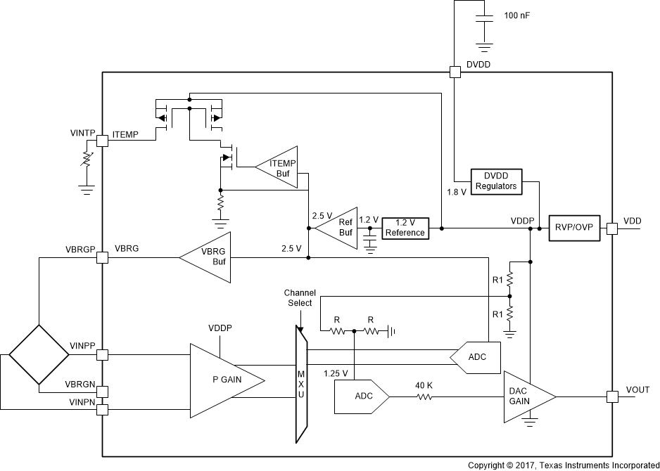 Figure 1. Bridge Supply and ADC Reference are Ratiometric
7.11 Bridge Offset Cancel
over operating free-air temperature range (unless otherwise noted)| PARAMETER | TEST CONDITIONS | MIN | TYP | MAX | UNIT | |
|---|---|---|---|---|---|---|
| Offset cancel range | –54.75 | +54.75 | mV | |||
| Offset cancel tolerance | –10% | +10% | ||||
| Offset cancel resolution (4 bits) | 10 | mV | ||||
7.12 P Gain and T Gain Input Amplifiers (Chopper Stabilized)
| PARAMETER | TEST CONDITIONS | MIN | TYP | MAX | UNIT | |
|---|---|---|---|---|---|---|
| Gain steps (3 bits) | 000, at DC | 1.31 | 1.33 | 1.35 | V/V | |
| 001 | 1.97 | 2 | 2.03 | |||
| 010 | 3.92 | 4 | 4.08 | |||
| 011 | 9.6 | 10 | 10.4 | |||
| 100 | 19 | 20 | 21 | |||
| 101 | 38 | 40 | 42 | |||
| 110 | 96 | 100 | 104 | |||
| 111 | 185 | 200 | 215 | |||
| Bandwidth | PGAIN = 1.33 | 680 | kHz | |||
| PGAIN = 2 | 470 | |||||
| PGAIN = 4 | 250 | |||||
| PGAIN = 10 | 104 | |||||
| PGAIN = 20 | 80 | |||||
| PGAIN = 40 | 72 | |||||
| PGAIN = 100 | 30 | |||||
| PGAIN = 200 | 15 | |||||
| Input offset voltage | 14 | µV | ||||
| Gain temperature drift | Gain = 200 V/V | –250 | +250 | ppm/°C | ||
| Input bias current | 5 | nA | ||||
| Common-mode voltage range | Depends on Selected Gain, Bridge Supply and Sensor Span (1) | V | ||||
| Common-mode rejection ratio | FCM = 50 Hz; ensured by design | 110 | dB | |||
| Input impedance | Ensured by design | 10 | MΩ | |||
(1) Common Mode at P Gain Input and Output:
- The single-ended voltage of positive/negative pin at the Gain input should be between +0.02 V and +4.38 V
7.13 Analog-to-Digital Converter
| PARAMETER | TEST CONDITIONS | MIN | TYP | MAX | UNIT | |
|---|---|---|---|---|---|---|
| Sigma delta modulator frequency | 4 | MHz | ||||
| ADC voltage input range | –2.5 | 2.5 | V | |||
| Number of bits | 16 | bits | ||||
| ADC 2's complement code for –2.5-V differential input | 2's Complement | 8000hex | LSB | |||
| ADC 2's complement code for 0-V differential input | 0000hex | LSB | ||||
| ADC 2's complement code for 2.5-V differential input | 7FFFhex | LSB | ||||
| Output sample period (no latency) | Sample period control bit = 0b00 | 96 | µs | |||
| ADC multiplexer switching time | 1 | µs | ||||
| Effective number of bits (ENOB) | Procedure to calculate ENOB:
|
11.4 | bits | |||
| ENOB in the presence of crosstalk between P and T channels | Procedure to calculate ENOB in the presence of crosstalk:
|
11.4 | bits | |||
| Linearity | Procedure to calculate Linearity:
|
±0.8 | %FS | |||
7.14 Internal Temperature Sensor
| PARAMETER | TEST CONDITIONS | MIN | TYP | MAX | UNIT | |
|---|---|---|---|---|---|---|
| Internal temperature sensor range | –40 | 150 | °C | |||
| Gain (1) | 16-bit ADC | 20 | LSB/°C | |||
| Offset | 5700 | LSB | ||||
| Total error after calibration using typical gain and offset values(2) | ±6 | °C | ||||
(1) ADC = Gain × Temperature + offset
(2) TI does not calibrate the sensor. User has to the calibrate the internal temperature sensor on their production line.
7.15 Bridge Current Measurement
| PARAMETER | TEST CONDITIONS | MIN | TYP | MAX | UNIT | |
|---|---|---|---|---|---|---|
| Bridge current range | 0 | 8500 | µA | |||
| Gain if T GAIN is configured for 1.33 Gain | 2250 | LSB/mA | ||||
| Offset T GAIN is configured for 1.33 Gain | 2075 | LSB | ||||
| Total temperature drift | Procedure to calculate Total Temperature Drift:
|
600 | ppm/°C | |||
7.16 One Wire Interface
| PARAMETER | TEST CONDITIONS | MIN | TYP | MAX | UNIT | |
|---|---|---|---|---|---|---|
| Communication baud rate | 2400 | 9600 | bits per second |
|||
| OWI_ENH | OWI activation high | OWI_ENL | V | |||
| OWI_ENL | OWI activation low | 6.8 | V | |||
| OWI_LOW | Activation signal pulse low time | OWI_DGL_CNT_SEL = 0 | 1 | ms | ||
| OWI_DGL_CNT_SEL = 1 | 10 | |||||
| OWI_HIGH | Activation signal pulse high time | OWI_DGL_CNT_SEL = 0 | 1 | ms | ||
| OWI_DGL_CNT_SEL = 1 | 10 | |||||
| OWI_VIH | OWI transceiver Rx threshold for high | 5.3 | V | |||
| OWI_VIL | OWI transceiver Rx threshold for low | 4.7 | V | |||
| OWI_IOH | OWI transceiver Tx threshold for hIgh | 900 | 1300 | µA | ||
| OWI_IOL | OWI transceiver Tx threshold for low | 2 | 5 | µA | ||
7.17 DAC Output
| PARAMETER | TEST CONDITIONS | MIN | TYP | MAX | UNIT | |
|---|---|---|---|---|---|---|
| DAC Reference Voltage | Ratiometric Reference | 0.25 × Vddp | V | |||
| DAC Resolution | 14 | Bits | ||||
7.18 DAC Gain for DAC Output
| PARAMETER | TEST CONDITIONS | MIN | TYP | MAX | UNIT | |
|---|---|---|---|---|---|---|
| Buffer gain (see Figure 2) | 3.9 | 4 | 4.3 | V/V | ||
| Gain bandwidth product | No Load, No DACCAP, Nominal Gain | 1 | MHz | |||
| Offset error (includes DAC errors) | Calculate Gain Nonlinearity at VDD = 5 V and 25°C as follows:
|
±20 | mV | |||
| Gain nonliearity (includes DAC errors) | Calculate Gain Nonlinearity at VDD = 5 V and 25°C as follows:
|
±600 | µV | |||
| Total unadjusted error | Calculate Gain Nonlinearity at VDD = 5 V and 25°C as follows:
|
–2 | 2 | %FSO | ||
| Ratiometric error due to change in temperature and load current for DAC code = 819d to 15564d. | Calculate ratiometric error at VDD = 5 V and at DAC codes as follows:
|
–10 | 10 | mV | ||
| Ratiometric error due to change in VDD for DAC code = 819d to 15564d. | Calculate ratiometric error at DAC codes as follows:
|
–12 | 12 | mV | ||
| Settling time (first order response) | DAC Code 819d to 15564d step and CLOAD = 100 nF. Output is 99% of Final Value | 100 | µs | |||
| Zero code voltage | DAC code = 0000h, IDAC = 1 mA |
100(1) | mV | |||
| DAC code = 0000h, IDAC = 2.5 mA |
250 | mV | ||||
| Full code voltage | Output when DAC code is 3FFFh, IDAC = –1 mA |
Vddp – 0.15(1) | V | |||
| Output when DAC code is 3FFFh, IDAC = –2.5 mA |
Vddp – 0.28 | V | ||||
| Output current | DAC Code = 3FFFh , DAC Code = 0000h | ±2.5 | mA | |||
| Short circuit source current | DAC code = 3FFFh | 10 | 40 | mA | ||
| Short circuit sink current | DAC code = 0000h | 10 | 40 | mA | ||
| Output voltage noise (GAIN = 4X) | ƒ = 10 Hz to 1 KHz, VDD = 4.5 V, DAC code = 1FFFh, no capacitor on DACCAP pin, temperature = 25°C | 80 | µVpp | |||
| Pullup resistance | 2 | 47 | KΩ | |||
| Pulldown resistance | 2 | 47 | KΩ | |||
| Capacitance | 0.1 | 1000 | nF | |||
(1) See Figure for voltage output bands.
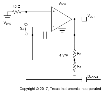 Figure 2. PGA302 Output Buffer
7.19 Non-Volatile Memory
| PARAMETER | TEST CONDITIONS | MIN | TYP | MAX | UNIT | |
|---|---|---|---|---|---|---|
| EEPROM | Size | 128 | Bytes | |||
| Erase/write cycles | 1000 | Cycles | ||||
| Programming time | 1 2-byte page | 8 | ms | |||
| Data retention | 10 | Years | ||||
7.20 Diagnostics - PGA30x
| PARAMETER | TEST CONDITIONS | MIN | TYP | MAX | UNIT | |
|---|---|---|---|---|---|---|
| VBRG_OV | Resistive bridge sensor supply overvoltage threshold | 7.5% | VBRG | |||
| VBRG_UV | Resistive bridge sensor supply undervoltage threshold | –4% | VBRG | |||
| VDD_OV | VDD OV threshold | 5.51 | V | |||
| DVDD_OV | DVDD OV threshold | 1.85 | V | |||
| REF_OV | Reference overvoltage threshold | 2.69 | V | |||
| REF_UV | Reference undervoltage threshold | 2.42 | V | |||
| P_DIAG_PD | Gain input diagnostics pulldown resistor value | VINPP and VINPN each has pulldown resistor | 1 | MΩ | ||
| 2 | ||||||
| 3 | ||||||
| 4 | ||||||
| T_DIAG_PD | T gain input diagnostics pulldown resistor value | VINTP and VINTN each has pulldown resistor | 1 | MΩ | ||
| VINP_OV | P gain input overvotlage threshold value | VINPP and VINPN each has threshold comparator | 90% | VBRDG | ||
| 84% | ||||||
| 78% | ||||||
| 70% | ||||||
| VINP_UV | P gain input undervotlage threshold value | VINPP and VINPN each has threshold comparator | 10% | VBRDG | ||
| 16% | ||||||
| 24% | ||||||
| 30% | ||||||
| VINT_OV | T gain input overvoltage | VINTP and VINTN | 90% | VBRG | ||
| VINT_UV | T gain input undervotlage | 10% | VBRG | |||
| PGAIN_OV | P gain output overvoltage | 2.5 | V | |||
| PGAIN_UV | P gain output undervoltage | 0.95 | V | |||
| TGAIN_OV | T gain output overvoltage | 2.5 | V | |||
| TGAIN_UV | T gain output undervoltage | 0.67 | V | |||
| HARNESS FAULT1 | Open wire VOUT voltage - open VDD with pullup on VOUT | Pullup resistor is 2 KΩ to 47 KΩ ±5%. across temperature | 5% | VDD | ||
| HARNESS_ FAULT2 |
Open wire VOUT voltage - open GND with pulldown on VOUT | Pulldown resistor is 2 KΩ to 47 KΩ ±5%, across temperature | 95% | VDD | ||
7.21 Typical Characteristics
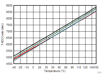 Figure 3. Internal Temperature Sensor
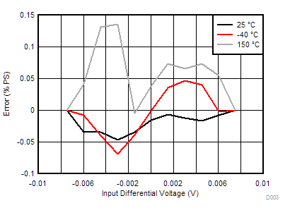 Figure 5. AFE and ADC Linearity Error
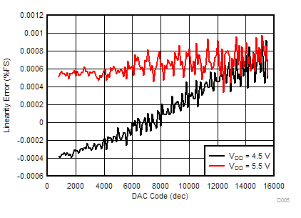 Figure 7. Ratiometric Error vs VDD Supply
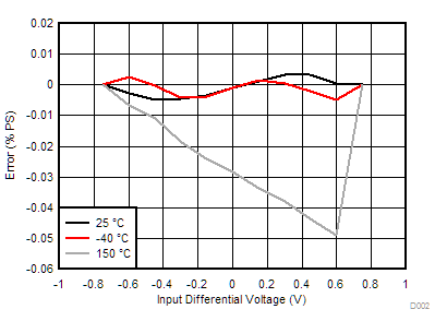 Figure 4. ADE and ADC Linearity Error
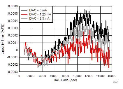 Figure 6. DAC Linearity Error
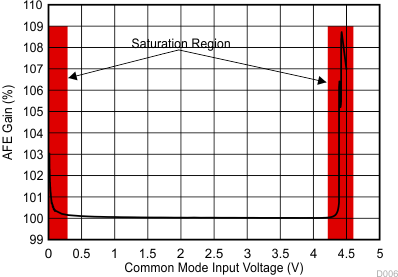 Figure 8. AFE Gain vs Common-Mode Input