SLTS278J November 2010 – March 2020 PTH08T250W
PRODUCTION DATA.
- 1 Features
- 2 Applications
- 3 Description
- 4 Revision History
- 5 Description (continued)
- 6 Pin Configuration and Functions
- 7 Specifications
- 8 Detailed Description
-
9 Application and Implementation
- 9.1
Typical Application
- 9.1.1
Detailed Design Procedure
- 9.1.1.1 Adjusting the Output Voltage
- 9.1.1.2
Capacitor Recommendations for the PTH08T250W Power Module
- 9.1.1.2.1 Capacitor Technologies
- 9.1.1.2.2 Input Capacitor (Required)
- 9.1.1.2.3 Input Capacitor Information
- 9.1.1.2.4 Output Capacitor (Required)
- 9.1.1.2.5 Output Capacitor Information
- 9.1.1.2.6 TurboTrans Output Capacitance
- 9.1.1.2.7 Non-TurboTrans Output Capacitance
- 9.1.1.2.8 Designing for Fast Load Transients
- 9.1.1.2.9 Capacitor Table
- 9.1.1.3 TurboTrans™ Technology
- 9.1.1.4 TurboTrans™ Selection
- 9.1.1.5 Undervoltage Lockout (UVLO)
- 9.1.1.6 On/Off Inhibit
- 9.1.1.7 Current Sharing
- 9.1.1.8 Prebias Startup Capability
- 9.1.1.9 SmartSync Technology
- 9.1.1.10 Auto-Track™ Function
- 9.1.1
Detailed Design Procedure
- 9.1
Typical Application
- 10Device and Documentation Support
- 11Mechanical, Packaging, and Orderable Information
Package Options
Refer to the PDF data sheet for device specific package drawings
Mechanical Data (Package|Pins)
- BCU|22
- ECT|22
- ECU|22
Thermal pad, mechanical data (Package|Pins)
Orderable Information
9.1.1.1 Adjusting the Output Voltage
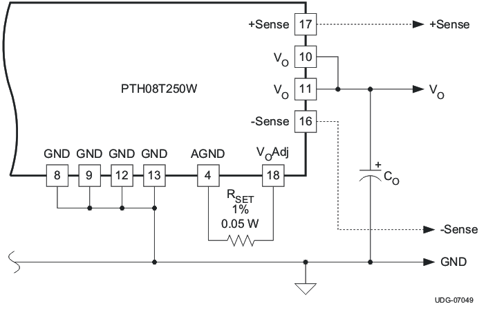
The Vo Adjust control sets the output voltage of the PTH08T250W. The adjustment range of the PTH08T250W is 0.7 V to 3.6 V. The adjustment method requires the addition of a single external resistor, RSET, that must be connected directly between pins Vo Adjust (pin 18) and AGND (pin 4). Table 2 gives the standard value of the external resistor for a number of standard voltages, along with the actual output voltage that this resistance value provides.
For other output voltages, the value of the required resistor can either be calculated using the following formula, or simply selected from the range of values given in Table 3. Figure 14 shows the placement of the required resistor.

Table 2. Standard Values of RSET for Standard Output Voltages
| VO (STANDARD) (V) | RSET (STANDARD VALUE) (kΩ) | VO (ACTUAL) (V) |
|---|---|---|
| 3.3 | 1.62 | 3.298 |
| 2.5 | 5.23 | 2.498 |
| 2.0 | 9.76 | 1.997 |
| 1.8 | 12.7 | 1.798 |
| 1.5 | 19.6 | 1.508 |
| 1.2 | 35.7 | 1.199 |
| 1.0 (1) | 63.4 | 1.001 |
| 0.7 (1) | Open | 0.700 |

Table 3. Output Voltage Set-Point Resistor Values
| VO REQUIRED (V) | RSET (kΩ) | VO REQUIRED (V) | RSET (kΩ) | VO REQUIRED (V) | RSET (kΩ) |
|---|---|---|---|---|---|
| 0.70 (1) | Open | 1.50 | 19.6 | 2.60 | 4.64 |
| 0.75 (1) | 412 | 1.60 | 16.9 | 2.70 | 4.02 |
| 0.80 (1) | 205 | 1.70 | 14.7 | 2.80 | 3.57 |
| 0.85 (1) | 133 | 1.80 | 12.7 | 2.90 | 3.09 |
| 0.90 (1) | 97.6 | 1.90 | 11.0 | 3.00 | 2.67 |
| 0.95 (1) | 78.7 | 2.00 | 9.76 | 3.10 | 2.26 |
| 1.00 (1) | 63.4 | 2.10 | 8.66 | 3.20 | 1.96 |
| 1.10 (1) | 46.4 | 2.20 | 7.50 | 3.30 | 1.62 |
| 1.20 | 35.7 | 2.30 | 6.65 | 3.40 | 1.30 |
| 1.30 | 28.7 | 2.40 | 5.90 | 3.50 | 1.02 |
| 1.40 | 23.7 | 2.50 | 5.23 | 3.60 | 0.768 |