SLLSEA0I February 2012 – January 2021 SN6501
PRODUCTION DATA
- 1 Features
- 2 Applications
- 3 Description
- 4 Pin Configuration and Functions
- 5 Specifications
- 6 Parameter Measurement Information
- 7 Detailed Description
- 8 Application and Implementation
- 9 Power Supply Recommendations
- 10Layout
- 11Device and Documentation Support
- 12Mechanical, Packaging, and Orderable Information
Package Options
Mechanical Data (Package|Pins)
- DBV|5
Thermal pad, mechanical data (Package|Pins)
Orderable Information
3 Description
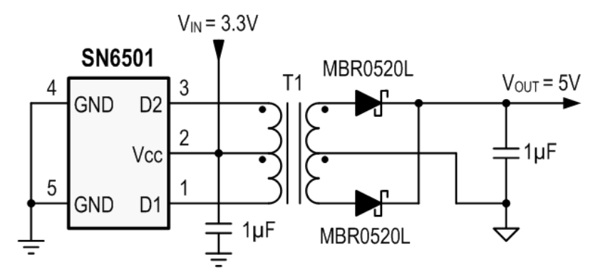
The SN6501 is a monolithic oscillator/power-driver, specifically designed for small form factor, isolated power supplies in isolated interface applications. The device drives a low-profile, center-tapped transformer primary from a 3.3-V or 5-V DC power supply. The secondary can be wound to provide any isolated voltage based on transformer turns ratio.
The SN6501 consists of an oscillator followed by a gate drive circuit that provides the complementary output signals to drive the ground referenced N-channel power switches. The internal logic ensures break-before-make action between the two switches.
The SN6501 is available in a small SOT-23 (5) package, and is specified for operation at temperatures from –40°C to 125°C.
| PART NUMBER(1) | PACKAGE | BODY SIZE (NOM) |
|---|---|---|
| SN6501 | SOT-23 (5) | 2.90 mm x 1.60 mm |
 Simplified Schematic.
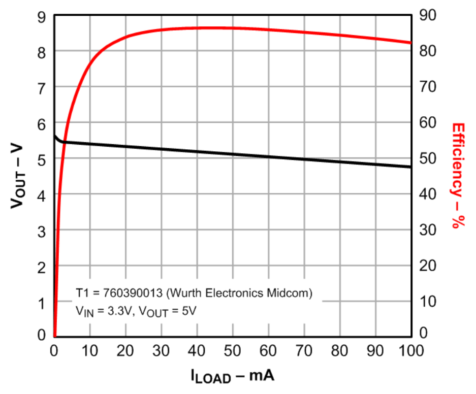
  Output Voltage and Efficiency vs Output Current.