SLLSEA0I February 2012 – January 2021 SN6501
PRODUCTION DATA
- 1 Features
- 2 Applications
- 3 Description
- 4 Pin Configuration and Functions
- 5 Specifications
- 6 Parameter Measurement Information
- 7 Detailed Description
- 8 Application and Implementation
- 9 Power Supply Recommendations
- 10Layout
- 11Device and Documentation Support
- 12Mechanical, Packaging, and Orderable Information
Package Options
Mechanical Data (Package|Pins)
- DBV|5
Thermal pad, mechanical data (Package|Pins)
Orderable Information
8.2.4 Higher Output Voltage Designs
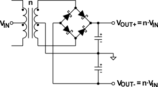
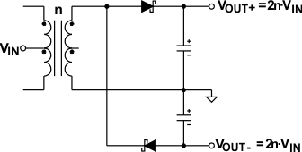
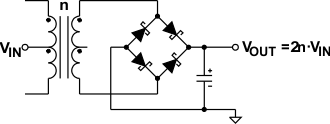
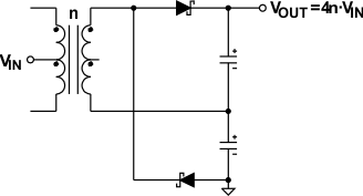
The SN6501 can drive push-pull converters that provide high output voltages of up to 30 V, or bipolar outputs of up to ±15 V. Using commercially available center-tapped transformers, with their rather low turns ratios of 0.8 to 5, requires different rectifier topologies to achieve high output voltages. Figure 8-8 to Figure 8-11 show some of these topologies together with their respective open-circuit output voltages.
 Figure 8-8 Bridge Rectifier With Center-Tapped Secondary Enables Bipolar Outputs
 Figure 8-10 Half-Wave Rectifier Without Center-Tapped Secondary Performs Voltage Doubling, Centered Ground Provides Bipolar Outputs
 Figure 8-9 Bridge Rectifier Without Center-Tapped Secondary Performs Voltage Doubling
 Figure 8-11 Half-Wave Rectifier Without Centered Ground and Center-Tapped Secondary Performs Voltage Doubling Twice, Hence Quadrupling VIN