SLLSEW9A December   2016  – June 2018 SN65DSI84-Q1

PRODUCTION DATA.  

  1. Features
  2. Applications
  3. Description
    1. 3.1 Typical Application
  4. Revision History
  5. Pin Configuration and Functions
    1.     Pin Functions
  6. Specifications
    1. 6.1 Absolute Maximum Ratings
    2. 6.2 ESD Ratings
    3. 6.3 Recommended Operating Conditions
    4. 6.4 Thermal Information
    5. 6.5 Electrical Characteristics
    6. 6.6 Switching Characteristics
  7. Parameter Measurement Information
  8. Detailed Description
    1. 8.1 Overview
    2. 8.2 Functional Block Diagram
    3. 8.3 Feature Description
      1. 8.3.1 Clock Configurations and Multipliers
      2. 8.3.2 ULPS
      3. 8.3.3 LVDS Pattern Generation
    4. 8.4 Device Functional Modes
      1. 8.4.1 Reset Implementation
      2. 8.4.2 Initialization Sequence
      3. 8.4.3 LVDS Output Formats
      4. 8.4.4 DSI Lane Merging
      5. 8.4.5 DSI Pixel Stream Packets
      6. 8.4.6 DSI Video Transmission Specifications
      7. 8.4.7 Operating Modes
    5. 8.5 Programming
      1. 8.5.1 Local I2C Interface Overview
    6. 8.6 Register Maps
      1. 8.6.1 Control and Status Registers Overview
        1. 8.6.1.1 CSR Bit Field Definitions – ID Registers
          1. 8.6.1.1.1 Registers 0x00 – 0x08
            1. Table 5. Registers 0x00 – 0x08 Field Descriptions
        2. 8.6.1.2 CSR Bit Field Definitions – Reset and Clock Registers
          1. 8.6.1.2.1 Register 0x09
            1. Table 6. Register 0x09 Field Descriptions
          2. 8.6.1.2.2 Register 0x0A
            1. Table 7. Register 0x0A Field Descriptions
          3. 8.6.1.2.3 Register 0x0B
            1. Table 8. Register 0x0B Field Descriptions
          4. 8.6.1.2.4 Register 0x0D
            1. Table 9. Register 0x0D Field Descriptions
        3. 8.6.1.3 CSR Bit Field Definitions – DSI Registers
          1. 8.6.1.3.1 Register 0x10
            1. Table 10. Register 0x10 Field Descriptions
          2. 8.6.1.3.2 Register 0x11
            1. Table 11. Register 0x11 Field Descriptions
          3. 8.6.1.3.3 Register 0x12
            1. Table 12. Register 0x12 Field Descriptions
        4. 8.6.1.4 CSR Bit Field Definitions – LVDS Registers
          1. 8.6.1.4.1 Register 0x18
            1. Table 13. Register 0x18 Field Descriptions
          2. 8.6.1.4.2 Register 0x19
            1. Table 14. Register 0x19 Field Descriptions
          3. 8.6.1.4.3 Register 0x1A
            1. Table 15. Register 0x1A Field Descriptions
          4. 8.6.1.4.4 Register 0x1B
            1. Table 16. Register 0x1B Field Descriptions
        5. 8.6.1.5 CSR Bit Field Definitions – Video Registers
          1. 8.6.1.5.1  Register 0x20
            1. Table 17. Register 0x20 Field Descriptions
          2. 8.6.1.5.2  Register 0x21
            1. Table 18. Register 0x21 Field Descriptions
          3. 8.6.1.5.3  Register 0x24
            1. Table 19. Register 0x24 Field Descriptions
          4. 8.6.1.5.4  Register 0x25
            1. Table 20. Register 0x25 Field Descriptions
          5. 8.6.1.5.5  Register 0x28
            1. Table 21. Register 0x28 Field Descriptions
          6. 8.6.1.5.6  Register 0x29
            1. Table 22. Register 0x29 Field Descriptions
          7. 8.6.1.5.7  Register 0x2C
            1. Table 23. Register 0x2C Field Descriptions
          8. 8.6.1.5.8  Register 0x2D
            1. Table 24. Register 0x2D Field Descriptions
          9. 8.6.1.5.9  Register 0x30
            1. Table 25. Register 0x30 Field Descriptions
          10. 8.6.1.5.10 Register 0x31
            1. Table 26. Register 0x31 Field Descriptions
          11. 8.6.1.5.11 Register 0x34
            1. Table 27. Register 0x34 Field Descriptions
          12. 8.6.1.5.12 Register 0x36
            1. Table 28. Register 0x36 Field Descriptions
          13. 8.6.1.5.13 Register 0x38
            1. Table 29. Register 0x38 Field Descriptions
          14. 8.6.1.5.14 Register 0x3A
            1. Table 30. Register 0x3A Field Descriptions
          15. 8.6.1.5.15 Register 0x3C
            1. Table 31. Register 0x3C Field Descriptions
        6. 8.6.1.6 CSR Bit Field Definitions – IRQ Registers
          1. 8.6.1.6.1 Register 0xE0
            1. Table 32. Register 0xE0 Field Descriptions
          2. 8.6.1.6.2 Register 0xE1
            1. Table 33. Register 0xE1 Field Descriptions
          3. 8.6.1.6.3 Register 0xE5
            1. Table 34. Register 0xE5 Field Descriptions
  9. Application and Implementation
    1. 9.1 Application Information
      1. 9.1.1 Video Stop and Restart Sequence
      2. 9.1.2 Reverse LVDS Pin Order Option
      3. 9.1.3 IRQ Usage
    2. 9.2 Typical Application
      1. 9.2.1 Design Requirements
      2. 9.2.2 Detailed Design Procedure
        1. 9.2.2.1 Example Script
      3. 9.2.3 Application Curve
  10. 10Power Supply Recommendations
    1. 10.1 VCC Power Supply
    2. 10.2 VCORE Power Supply
  11. 11Layout
    1. 11.1 Layout Guidelines
      1. 11.1.1 Package Specific
      2. 11.1.2 Differential Pairs
      3. 11.1.3 Ground
    2. 11.2 Layout Example
  12. 12Device and Documentation Support
    1. 12.1 Documentation Support
      1. 12.1.1 Related Documentation
    2. 12.2 Receiving Notification of Documentation Updates
    3. 12.3 Community Resources
    4. 12.4 Trademarks
    5. 12.5 Electrostatic Discharge Caution
    6. 12.6 Glossary
  13. 13Mechanical, Packaging, and Orderable Information

Package Options

Mechanical Data (Package|Pins)
Thermal pad, mechanical data (Package|Pins)
Orderable Information

Description

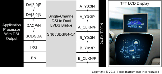
The SN65DSI84-Q1 DSI-to-LVDS bridge features a single-channel MIPI D-PHY receiver front-end configuration with four lanes per channel operating at 1 Gbps per lane and a maximum input bandwidth of 4 Gbps. The bridge decodes MIPI® DSI 18-bpp RGB666 and 24-bpp RGB888 packets and converts the formatted video data-stream to an LVDS output operating at pixel clocks operating from 25 MHz to 154 MHz, offering a dual-link LVDS or single-link LVDS with four data lanes per link.

The SN65DSI84-Q1 device is well suited for WUXGA (1920 × 1080) at 60 frames per second (fps) with up to 24 bits-per-pixel (bpp). Partial line buffering is implemented to accommodate the data stream mismatch between the DSI and LVDS interfaces.

The SN65DSI84-Q1 device is implemented in a small outline 10 mm × 10 mm HTQFP package with a
0.5-mm pitch, and operates across a temperature range from –40°C to 105°C.

Device Information(1)

PART NUMBER PACKAGE BODY SIZE (NOM)
SN65DSI84-Q1 HTQFP (64) 10.00 mm × 10.00 mm
  1. For all available packages, see the orderable addendum at the end of the data sheet.

Typical Application

SN65DSI84-Q1 alt_sllsew9.gif