SLLS666F September 2005 – March 2023 SN65HVD50 , SN65HVD52 , SN65HVD53 , SN65HVD54 , SN65HVD55
PRODUCTION DATA
- 1 Features
- 2 Applications
- 3 Description
- 4 Revision History
- 5 Available Options
- 6 Pin Configurations
-
7 Specifications
- 7.1 Absolute Maximum Ratings
- 7.2 Recommended Operating Conditions
- 7.3 Electrostatic Discharge Protection
- 7.4 Driver Electrical Characteristics
- 7.5 Driver Switching Characteristics
- 7.6 Receiver Electrical Characteristics
- 7.7 Receiver Switching Characteristics
- 7.8 Thermal Characteristics
- 7.9 Typical Characteristics
- 8 Parameter Measurement Information
- 9 Device Information
- 10Application and Implementation
- 11Device and Documentation Support
- 12Mechanical, Packaging, and Orderable Information
Package Options
Mechanical Data (Package|Pins)
- D|14
Thermal pad, mechanical data (Package|Pins)
- D|14
Orderable Information
7.9 Typical Characteristics
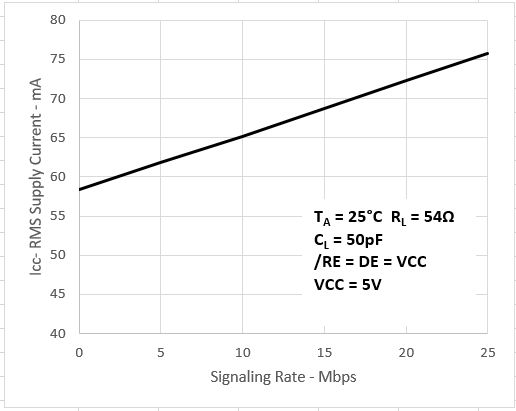 Figure 7-1 HVD50, HVD53 RMS Supply
Current
Figure 7-1 HVD50, HVD53 RMS Supply
Currentvs Signaling Rate
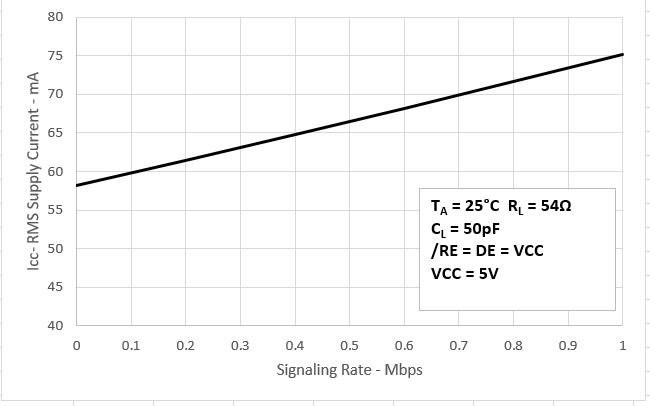 Figure 7-3 HVD52, HVD55 RMS Supply
Current
Figure 7-3 HVD52, HVD55 RMS Supply
Currentvs Signaling Rate
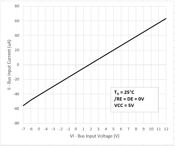 Figure 7-5 HVD51, HVD52, HVD54, HVD55
BUS Input Current
Figure 7-5 HVD51, HVD52, HVD54, HVD55
BUS Input Currentvs Input Voltage
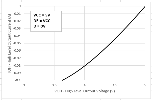 Figure 7-7 Driver High-Level Output
Current
Figure 7-7 Driver High-Level Output
Currentvs High-Level Output Voltage
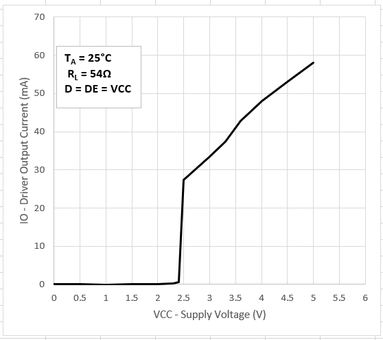 Figure 7-9 Driver Output Current vs
Supply Voltage
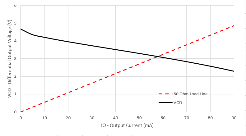 Figure 7-11 Diferential Output Voltage
vs Output Current
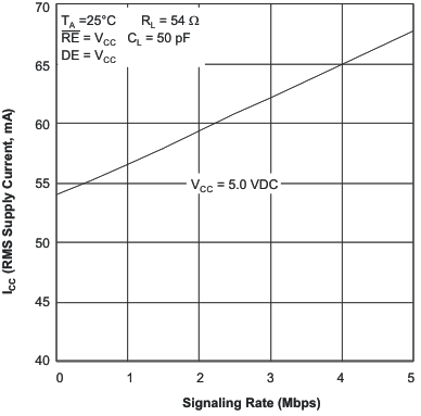 Figure 7-2 HVD51, HVD54 RMS Supply Current
vs Signaling Rate
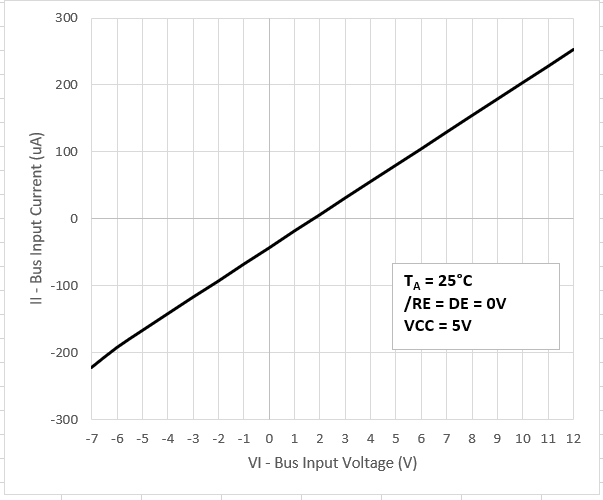 Figure 7-4 HVD50, HVD53 BUS Input
Current vs Input Voltage
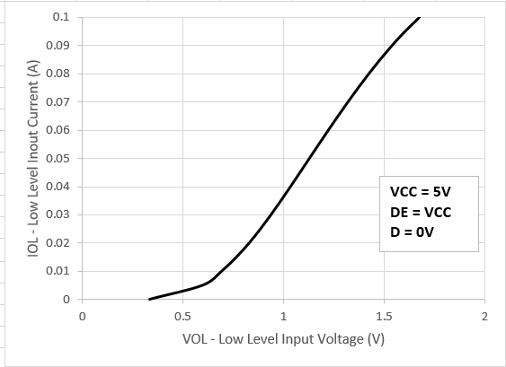 Figure 7-6 Driver LOW-Level Output
Current
Figure 7-6 Driver LOW-Level Output
Currentvs Low-Level Output Voltage
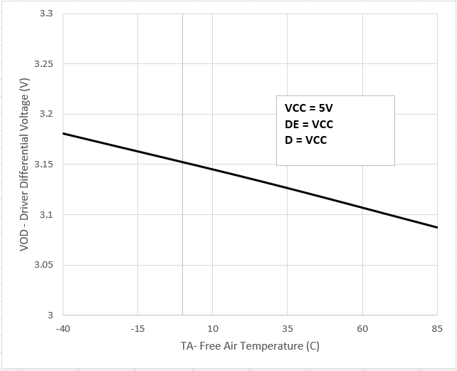 Figure 7-8 Driver Differential Output
Voltage
Figure 7-8 Driver Differential Output
Voltagevs Free-Air Temperature
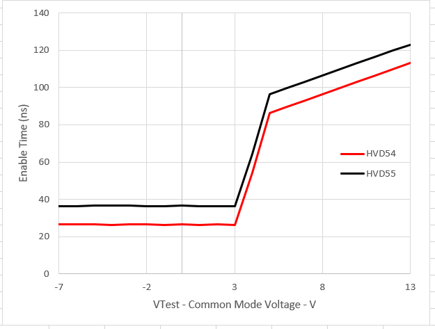 Figure 7-10 Enable Time vs Common-Mode
Voltage
Figure 7-10 Enable Time vs Common-Mode
Voltage(See Figure 7-12)
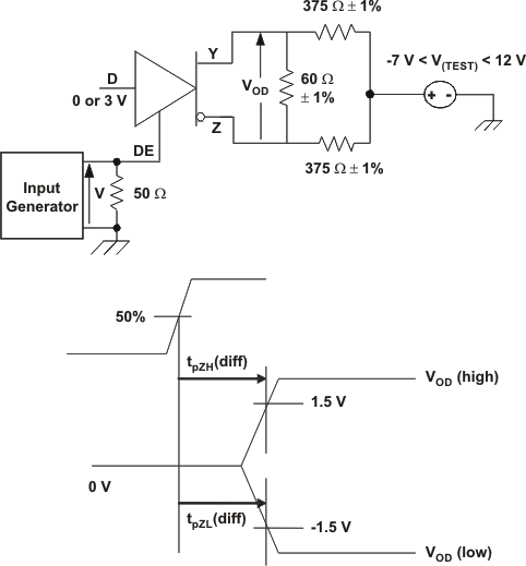
- The time tpZL(x) is the measure from DE to VOD(x). VOD is valid when it is greater than 1.5 V.