SLLS666F September 2005 – March 2023 SN65HVD50 , SN65HVD52 , SN65HVD53 , SN65HVD54 , SN65HVD55
PRODUCTION DATA
- 1 Features
- 2 Applications
- 3 Description
- 4 Revision History
- 5 Available Options
- 6 Pin Configurations
-
7 Specifications
- 7.1 Absolute Maximum Ratings
- 7.2 Recommended Operating Conditions
- 7.3 Electrostatic Discharge Protection
- 7.4 Driver Electrical Characteristics
- 7.5 Driver Switching Characteristics
- 7.6 Receiver Electrical Characteristics
- 7.7 Receiver Switching Characteristics
- 7.8 Thermal Characteristics
- 7.9 Typical Characteristics
- 8 Parameter Measurement Information
- 9 Device Information
- 10Application and Implementation
- 11Device and Documentation Support
- 12Mechanical, Packaging, and Orderable Information
Package Options
Mechanical Data (Package|Pins)
- D|14
Thermal pad, mechanical data (Package|Pins)
- D|14
Orderable Information
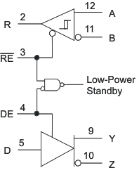
9.1 Ll-Power Standby Mode
When both the driver and receiver are disabled (DE low and RE high) the device is in standby mode. If the enable inputs are in this state for less than 60 ns, the device does not enter standby mode. This guards against inadvertently entering standby mode during driver/receiver enabling. Only when the enable inputs are held in this state for 300 ns or more, the device is assured to be in standby mode. In this low-power standby mode, most internal circuitry is powered down, and the supply current is typically less than 1 nA. When either the driver or the receiver is re-enabled, the internal circuitry becomes active.
 Figure 9-1 Low-Power Standby Logic Diagram
If only the driver is re-enabled (DE transitions to high) the driver outputs are driven according to the D input after the enable times given by tPZH2 and tPZL2 in the driver switching characteristics. If the D input is open when the driver is enabled, the driver outputs defaults to A high and B low, in accordance with the driver failsafe feature.
If only the receiver is re-enabled ( RE transitions to low) the receiver output is driven according to the state of the bus inputs (A and B) after the enable times given by tPZH2 and tPZL2 in the receiver switching characteristics. If there is no valid state on the bus the receiver responds as described in the failsafe operation section.
If both the receiver and driver are re-enabled simultaneously, the receiver output is driven according to the state of the bus inputs (A and B) and the driver output is driven according to the D input. Note that the state of the active driver affects the inputs to the receiver. Therefore, the receiver outputs are valid as soon as the driver outputs are valid.