SCES551E February   2004  – November 2015 SN74AVC16T245

PRODUCTION DATA.  

  1. Features
  2. Applications
  3. Description
  4. Revision History
  5. Description (continued)
  6. Pin Configuration and Functions
  7. Specifications
    1. 7.1  Absolute Maximum Ratings
    2. 7.2  ESD Ratings
    3. 7.3  Recommended Operating Conditions
    4. 7.4  Thermal Information
    5. 7.5  Electrical Characteristics
    6. 7.6  Switching Characteristics: VCCA = 1.2 V
    7. 7.7  Switching Characteristics: VCCA = 1.5 V ± 0.1 V
    8. 7.8  Switching Characteristics: VCCA = 1.8 V ± 0.15 V
    9. 7.9  Switching Characteristics: VCCA = 2.5 V ± 0.2 V
    10. 7.10 Switching Characteristics: VCCA = 3.3 V ± 0.3 V
    11. 7.11 Operating Characteristics
    12. 7.12 Typical Characteristics
  8. Parameter Measurement Information
  9. Detailed Description
    1. 9.1 Overview
    2. 9.2 Functional Block Diagram
    3. 9.3 Feature Description
      1. 9.3.1 Fully Configurable Dual-Rail Design Allows Each Port to Operate Over the Full 1.2-V to 3.6-V Power-Supply Range
      2. 9.3.2 Partial-Power-Down Mode Operation
      3. 9.3.3 VCC Isolation
    4. 9.4 Device Functional Modes
  10. 10Application and Implementation
    1. 10.1 Application Information
      1. 10.1.1 Enable Times
    2. 10.2 Typical Application
      1. 10.2.1 Design Requirements
      2. 10.2.2 Detailed Design Procedure
        1. 10.2.2.1 Input Voltage Ranges
        2. 10.2.2.2 Output Voltage Range
      3. 10.2.3 Application Curve
  11. 11Power Supply Recommendations
  12. 12Layout
    1. 12.1 Layout Guidelines
    2. 12.2 Layout Example
  13. 13Device and Documentation Support
    1. 13.1 Documentation Support
      1. 13.1.1 Related Documentation
    2. 13.2 Community Resources
    3. 13.3 Trademarks
    4. 13.4 Electrostatic Discharge Caution
    5. 13.5 Glossary
  14. 14Mechanical, Packaging, and Orderable Information

Package Options

Mechanical Data (Package|Pins)
Thermal pad, mechanical data (Package|Pins)
Orderable Information

6 Pin Configuration and Functions

GQL or ZQL Package
56-Pin BGA MICROSTAR JUNIOR
Top View
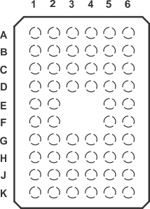
SN74AVC16T245 gql_ces551.gif
DGG or DGV Package
48-Pin TSSOP or TVSOP
Top View
SN74AVC16T245 po_ces551.gif

Pin Functions

PIN I/O DESCRIPTION
NAME TSSOP,
TVSOP
BGA MICROSTAR
1DIR, 2DIR 1, 24 A1, K1 I Direction-control signal
1B1 to 1B8 2, 3, 5, 6, 8, 9, 11, 12 B2, B1, C2, C1, D2, D1, E2, E1 I/O Input/Output. Referenced to VCCB
2B1 to 2B8 13, 14, 16, 17, 19, 20, 22, 23 F1, F2, G1, G2, H1, H2, J1, J2 I/O Input/Output. Referenced to VCCB
GND 4, 10, 15, 21, 45, 39, 34, 28 B3, D3, G3, J3, J4, G4, D4, B4 Ground
VCCB 7, 18 C3, H3 B-port supply voltage. 1.2 V ≤ VCCB ≤ 3.6 V
1OE, 2OE 48, 25 A6, K6 Tri-State output-mode enables. Pull OE high to place all outputs in Tri-State mode. Referenced to VCCA
1A1 to 1A8 47, 46, 44, 43, 41, 40, 38, 37 B5, B6, C5, C6, D5, D6, E5, E6 I/O Input/Output. Referenced to VCCA
2A1 to 2A8 36, 35, 33, 32, 30, 29, 27, 26 F6, F5, G6, G5, H6, H5, J6, J5 I/O Input/Output. Referenced to VCCA
VCCA 42, 31 C4, H4 A-port supply voltage. 1.2 V ≤ VCCB ≤ 3.6 V
N.C. A2, A3, A4, A5, K2, K3, K4, K5 No internal connection