SLLS059E February 1990 – February 2024 SN751177 , SN751178
PRODUCTION DATA
- 1
- 1 Features
- 2 Applications
- 3 Description
- 4 Pin Configuration and Functions
- 5 Specifications
- 6 Parameter Measurement Information
- 7 Detailed Description
- 8 Device and Documentation Support
- 9 Revision History
- 10Mechanical, Packaging, and Orderable Information
Package Options
Refer to the PDF data sheet for device specific package drawings
Mechanical Data (Package|Pins)
- NS|16
- N|16
Thermal pad, mechanical data (Package|Pins)
Orderable Information
6 Parameter Measurement Information
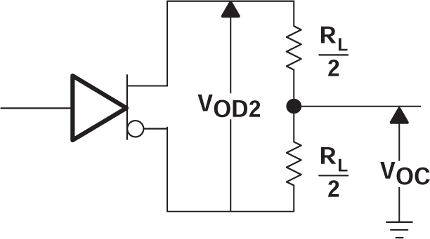
 Figure 6-1 Driver Test Circuit, vOD And vOC
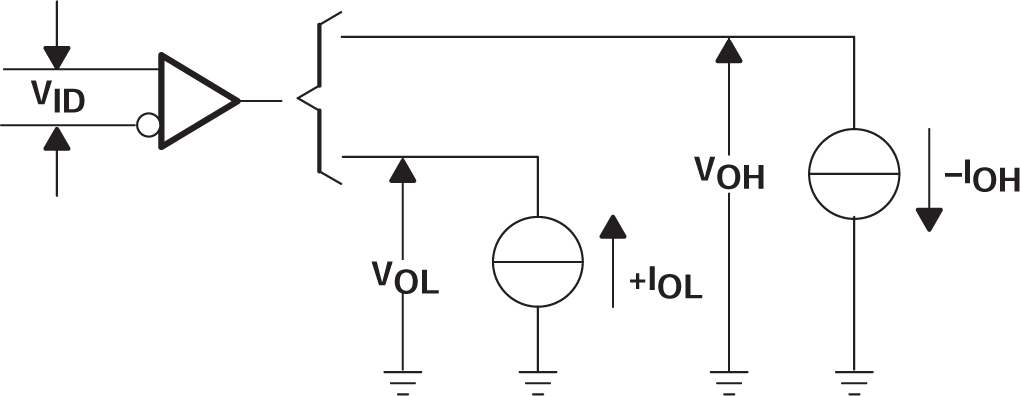
 Figure 6-2 Receiver Test Circuit, vOH And vOL

A. CL includes probe and jig capacitance.
B. The pulse generator
has the following characteristics: PRR ≤ 1MHz, 50% duty cycle, ZO =
50Ω, tr ≤ 6ns, tf ≤ 6ns.
Figure 6-3 Driver Differential Output-Delay and Transition-Time Test Circuit and Voltage Waveforms
A. CL includes probe and jig capacitance.
B. The pulse generator
has the following characteristics: PRR ≤ 1MHz, 50% duty cycle, ZO =
50Ω, tr ≤ 6ns, tf ≤ 6ns.
Figure 6-4 Driver Propagation-Time Test Circuit and Voltage Waveforms
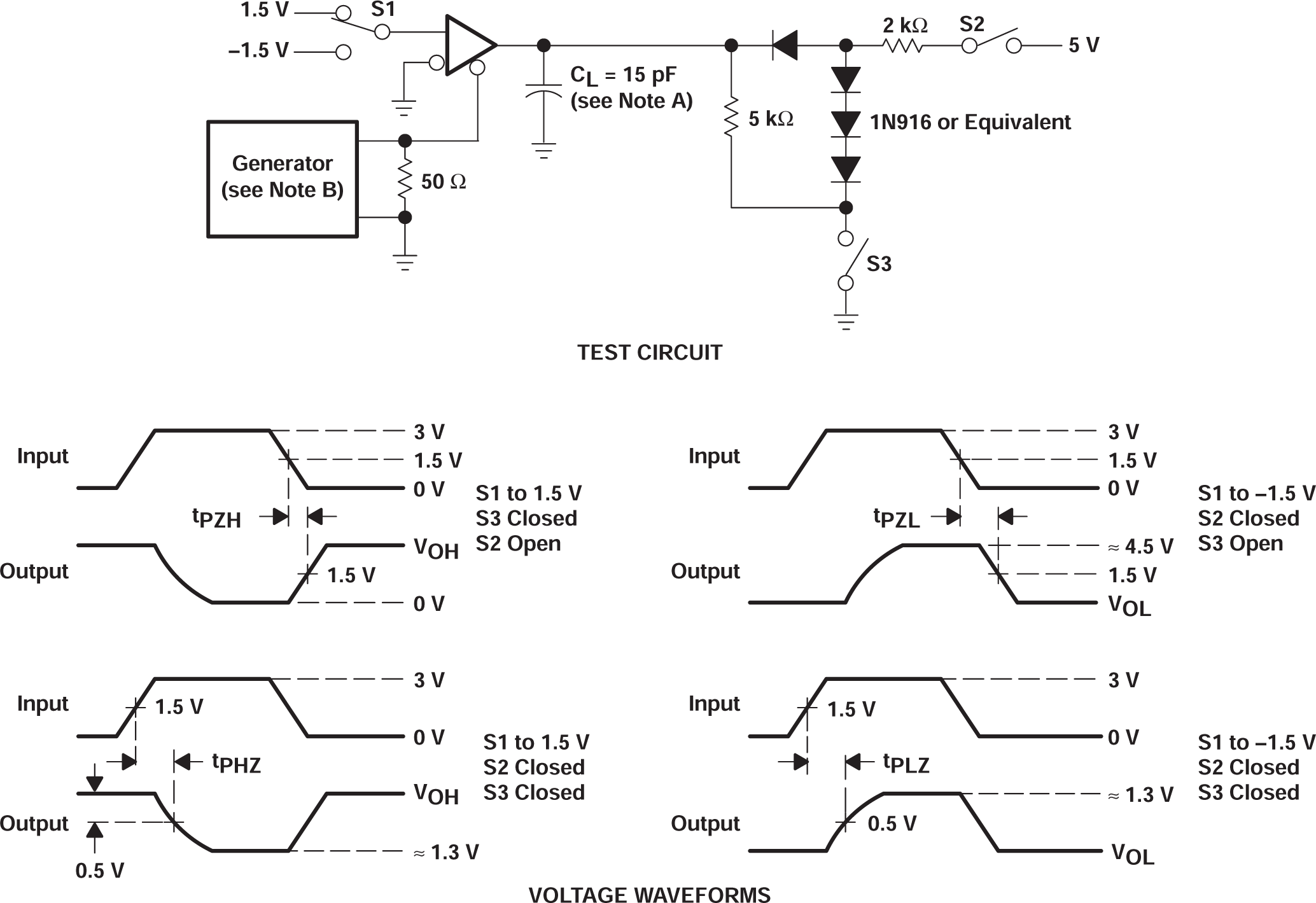
A. CL includes probe and jig capacitance.
B. The pulse generator
has the following characteristics: PRR ≤ 1MHz, 50% duty cycle, ZO =
50Ω, tr ≤ 6ns, tf ≤ 6ns.
Figure 6-5 Driver Enable- and Disable-Time Test Circuit and Voltage Waveforms
A. CL includes probe and jig capacitance.
B. The pulse generator
has the following characteristics: PRR ≤ 1MHz, 50% duty cycle, ZO =
50Ω, tr ≤ 6ns, tf ≤ 6ns.
Figure 6-6 Driver Enable- and Disable-Time Test Circuit and Voltage Waveforms
A. CL includes probe and jig capacitance.
B. The pulse
generator has the following characteristics: PRR ≤ 1MHz, 50% duty cycle,
ZO = 50Ω, tr ≤ 6ns, tf ≤ 6ns.
Figure 6-7 Receiver Propagation-Time Test Circuit and Voltage Waveforms
A. CL includes probe and jig capacitance.
B. The pulse
generator has the following characteristics: PRR ≤ 1MHz, 50% duty cycle,
ZO = 50Ω, tr ≤ 6ns, tf ≤ 6ns.
Figure 6-8 Receiver Output Enable- and Disable-Time Test Circuit and Voltage Waveforms