SLLS059E February 1990 – February 2024 SN751177 , SN751178
PRODUCTION DATA
- 1
- 1 Features
- 2 Applications
- 3 Description
- 4 Pin Configuration and Functions
- 5 Specifications
- 6 Parameter Measurement Information
- 7 Detailed Description
- 8 Device and Documentation Support
- 9 Revision History
- 10Mechanical, Packaging, and Orderable Information
Package Options
Refer to the PDF data sheet for device specific package drawings
Mechanical Data (Package|Pins)
- NS|16
- N|16
Thermal pad, mechanical data (Package|Pins)
Orderable Information
4 Pin Configuration and Functions
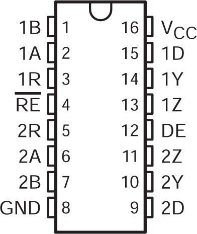
 Figure 4-1 SN751177: N or NS Package
(Top View)
| PIN | TYPE | DESCRIPTION | ||
|---|---|---|---|---|
| NAME | PDIP | SO | ||
| 1A | 2 | 2 | I | RS422 differential input (non-inverting) to receiver 1 |
| 2A | 6 | 6 | I | RS422 differential input (non-inverting) to receiver 2 |
| 1B | 1 | 1 | I | RS422 differential input (inverting) to receiver 1 |
| 2B | 7 | 7 | I | RS422 differential input (inverting) to receiver 2 |
| 1D | 15 | 15 | I | Logic data input to RS422 driver 1 |
| 2D | 9 | 9 | I | Logic data input to RS422 driver 2 |
| DE | 12 | 12 | I | Driver enable (active high) |
| GND | 8 | 8 | — | Device ground pin |
| 1R | 3 | 3 | O | Logic data output of RS422 receiver 1 |
| 2R | 5 | 5 | O | Logic data output of RS422 receiver 2 |
| RE | 4 | 4 | I | Receiver enable pin (active low) |
| VCC | 16 | 16 | — | Power supply |
| 1Y | 14 | 14 | O | RS-422 differential (non-inverting) driver output 1 |
| 2Y | 10 | 10 | O | RS-422 differential (non-inverting) driver output 2 |
| 1Z | 13 | 13 | O | RS-422 differential (inverting) driver output 1 |
| 2Z | 11 | 11 | O | RS-422 differential (inverting) driver output 2 |
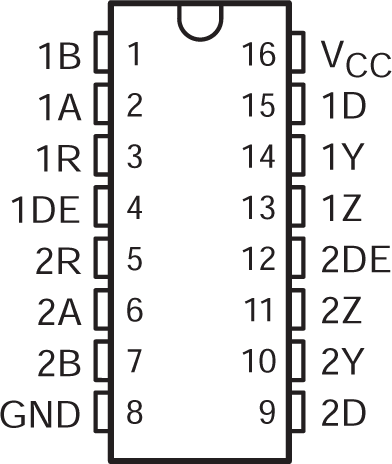
 Figure 4-2 SN751178: N or NS Package
(Top View)
| PIN | TYPE | DESCRIPTION | ||
|---|---|---|---|---|
| NAME | PDIP | SO | ||
| 1A | 2 | 2 | I | RS422 differential input (non-inverting) to receiver 1 |
| 2A | 6 | 6 | I | RS422 differential input (non-inverting) to receiver 2 |
| 1B | 1 | 1 | I | RS422 differential input (inverting) to receiver 1 |
| 2B | 7 | 7 | I | RS422 differential input (inverting) to receiver 2 |
| 1D | 15 | 15 | I | Logic data input to RS422 driver 1 |
| 2D | 9 | 9 | I | Logic data input to RS422 driver 2 |
| 1DE | 4 | 4 | I | Driver 1 enable (active high) |
| 2DE | 12 | 12 | I | Driver 2 enable (active high) |
| GND | 8 | 8 | — | Device ground |
| 1R | 3 | 3 | O | Logic data output of RS422 receiver 1 |
| 2R | 5 | 5 | O | Logic data output of RS422 receiver 2 |
| VCC | 16 | 16 | — | Power supply |
| 1Y | 14 | 14 | O | RS-422 differential (non-inverting) driver output 1 |
| 2Y | 10 | 10 | O | RS-422 differential (non-inverting) driver output 2 |
| 1Z | 13 | 13 | O | RS-422 differential (non inverting) driver output 1 |
| 2Z | 11 | 11 | O | RS-422 differential (non inverting) driver output 2 |