SLLS059E February 1990 – February 2024 SN751177 , SN751178
PRODUCTION DATA
- 1
- 1 Features
- 2 Applications
- 3 Description
- 4 Pin Configuration and Functions
- 5 Specifications
- 6 Parameter Measurement Information
- 7 Detailed Description
- 8 Device and Documentation Support
- 9 Revision History
- 10Mechanical, Packaging, and Orderable Information
Package Options
Refer to the PDF data sheet for device specific package drawings
Mechanical Data (Package|Pins)
- NS|16
- N|16
Thermal pad, mechanical data (Package|Pins)
Orderable Information
3 Description
The SN751177 and SN751178 dual differential drivers and receivers are monolithic integrated circuits that are designed for balanced multipoint bus transmission at rates up to 10 Mbits. The devices are designed to improve the performance of full-duplex data communications over long bus lines and meet ANSI Standards TIA/EIA-422-B and TIA/EIA-485-A and ITU Recommendations V.10 and V.11.
The SN751177 and SN751178 driver outputs provide limiting for both positive and negative currents and thermal-shutdown protection from line-fault conditions on the transmission bus line.
The receiver features high input impedance of at least 12kΩ, an input sensitivity of ±200mV over a common-mode input voltage range of −12V to 12V, and typical input hysteresis of 50mV. Fail-safe design makes sure the receiver inputs are open, the receiver outputs are always high.
The SN751177 and SN751178 are characterized for operation from −20°C to 85°C.
| PART NUMBER | PACKAGE(1) | PACKAGE SIZE(2) |
|---|---|---|
| SN751177 SN751178 | PDIP (N, 16) | 19.3mm × 9.4mm |
| SO (NS, 16) | 10.2mm × 7.8mm |
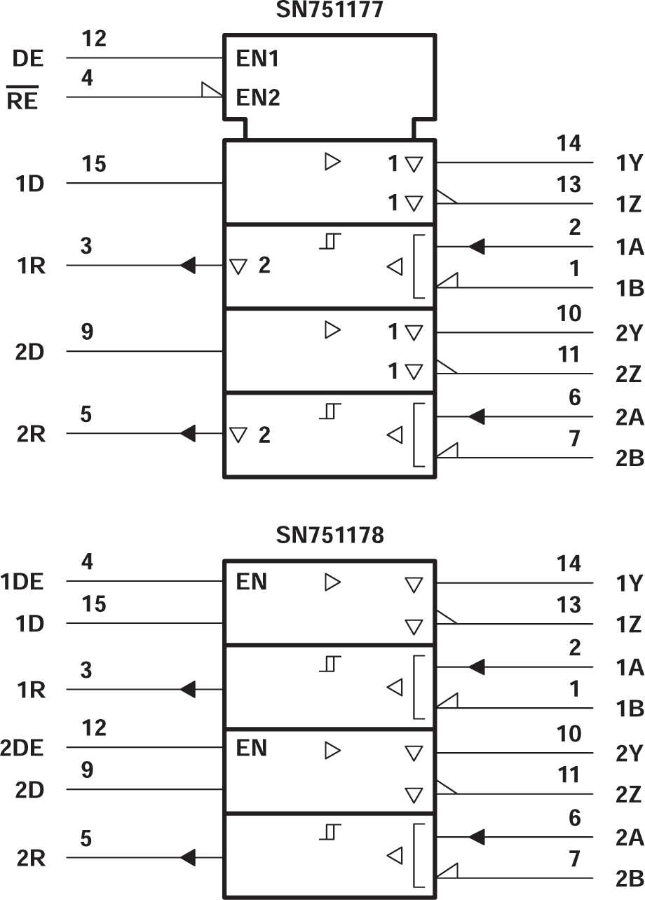
 Logic Symbols(1)
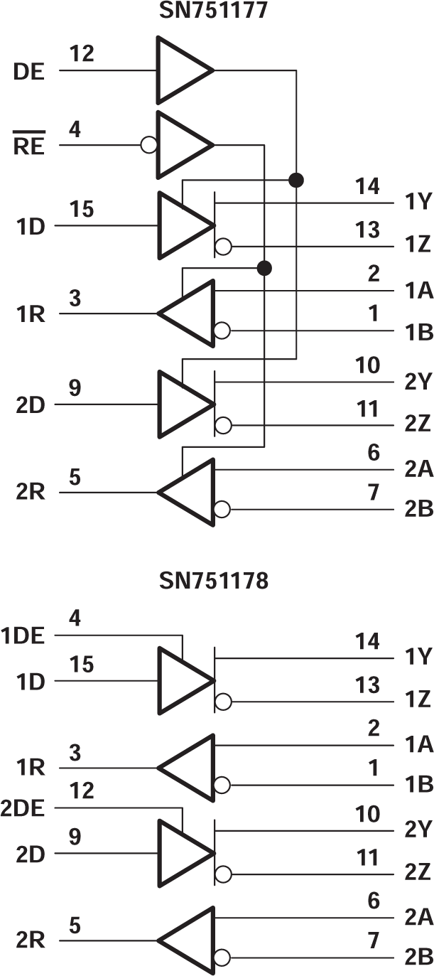
 Logic Diagrams (Positive Logic)