SLLSE12A November 2009 – July 2014 SN75DP119
PRODUCTION DATA.
- 1 Features
- 2 Applications
- 3 Description
- 4 Revision History
- 5 Description (continued)
- 6 Pin Configuration and Functions
- 7 Specifications
- 8 Parameter Measurement Information
- 9 Detailed Description
- 10Application and Implementation
- 11Power Supply Recommendations
- 12Layout
- 13Device and Documentation Support
- 14Mechanical, Packaging, and Orderable Information
Package Options
Mechanical Data (Package|Pins)
Thermal pad, mechanical data (Package|Pins)
Orderable Information
1 Features
2 Applications
- eDP
- Desktop PC
- Notebook PC
- PC Docking Station
- PC Standalone Video Card
3 Description
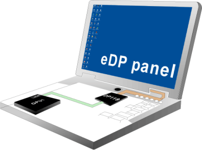
The SN75DP119 is a 1-lane or 2-lane embedded DisplayPort (eDP) repeater that regenerates the DP high speed digital link. The device compensates for pcb related frequency loss and signal reflections. This is especially helpful in designs with long pcb traces or when there is a FET switch in the signal path.
Four levels of differential output voltage swing (VOD) and any combination of pre-emphasis using these VOD levels are supported. The output swing and pre-emphasis are configured through device control inputs. The available output swing levels are 300mVPP, 400mVPP, 600mVPP or 750mVPP. Therefore, the output pre-emphasis level can be configured to 0dB, 2.0dB, 2,5dB, 3.5dB, 5.5dB, 6dB, or 8dB. This is a good solution for embedded link applications, such as the connection from the GPU to the notebook internal panel. To adjust the output signal level adaptively during link training, the implementation needs to control the device control inputs.
The SN75DP119 supports programmable integrated receiver equalization circuitry. This equalization circuitry can be used to help improve signal integrity in applications where the input link has a high level of insertion loss. The equalizer can be set to 3dB or 6dB equalization. The equalizer can also be turned off.
Device Information(1)
| PART NUMBER | PACKAGE | BODY SIZE (NOM) |
|---|---|---|
| SN75DP119 | VQFN (14) | 3.50mm x 3.50mm |
| VQFN (36) | 6.00mm x 6.00mm |
- For all available packages, see the orderable addendum at the end of the datasheet.