SLLSE12A November 2009 – July 2014 SN75DP119
PRODUCTION DATA.
- 1 Features
- 2 Applications
- 3 Description
- 4 Revision History
- 5 Description (continued)
- 6 Pin Configuration and Functions
- 7 Specifications
- 8 Parameter Measurement Information
- 9 Detailed Description
- 10Application and Implementation
- 11Power Supply Recommendations
- 12Layout
- 13Device and Documentation Support
- 14Mechanical, Packaging, and Orderable Information
Package Options
Mechanical Data (Package|Pins)
Thermal pad, mechanical data (Package|Pins)
Orderable Information
6 Pin Configuration and Functions
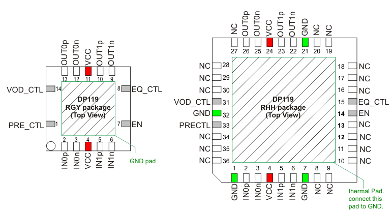
Pin Functions, RGY Package
| PIN | DESCRIPTION | ||
|---|---|---|---|
| NAME | NUMBER | I/O | |
| MAIN LINK INPUT PINS | |||
| IN0p | 2 | I [100Ω diff] | DisplayPort Main Link Channel 0 Differential Input |
| IN0n | 3 | ||
| IN1p | 5 | DisplayPort Main Link Channel 1 Differential Input | |
| IN1n | 6 | ||
| MAIN LINK OUTPUT PINS | |||
| OUT0p | 13 | O [100Ω diff] | DisplayPort Main Link Channel 0 Differential Output |
| OUT0n | 12 | ||
| OUT1p | 10 | DisplayPort Main Link Channel 1 Differential Output | |
| OUT1n | 9 | ||
| CONTROL PINS | |||
| EN | 7 | 3-level Input [CMOS] |
Enable. This input is a 3-level input. If the input is left open, the internal input biasing pulls the input level to VCC/2. The input can also be pulled high or low externally. This allows to configure the device for 1-channel mode, 2-channel mode or power down mode. |
| EN = HIGH: Device in Normal Mode, both outputs OUT1 and OUT2 are enabled; EN = VCC/2 (input left floating): Device in Normal mode, 2nd output is disabled; EN = LOW: Device in Power Down mode. All outputs are high-impedance; Inputs are ignored |
|||
| PRE_CTL | 1 | 3-level Input [CMOS] |
Configures the output pre-emphasis level. This input is a 3-level input. If the input is left open, the internal input biasing pulls the input level to VCC/2. The input can also be pulled high or low externally. This allows to configure the pre-emphasis for 3 different levels. See Table 1 for configuration details. |
| VOD_CTL | 14 | 3-level Input [CMOS] |
Configures the output amplitude VOD level. This input is a 3-level input. If the input is left open, the internal input biasing pulls the input level to VCC/2. The input can also be pulled high or low externally. This allows to configure 3 different output swing amplitudes. See Table 1 for configuration details. |
| EQ_CTL | 8 | 3-level Input [CMOS] |
Configures the EQ input setting for both differential inputs. This input is a 3-level input. If the input is left open, the internal input biasing pulls the input level to VCC/2. The input can also be pulled high or low externally. This allows to configure the pre-emphasis for 3 different levels. |
| EQ_CTL = LOW: 0dB (EQ turned off) EQ_CTL = VCC/2 (input left floating): 3dB fixed EQ EQ_CTL = HIGH (input tied to VCC): 6dB fixed EQ |
|||
| SUPPLY AND GROUND PINS | |||
| VCC | 4, 11 | pwr | 3.3V Supply |
| GND | thermal pad | pwr | Ground |
| Note: (H) Logic High: (L) Logic Low | |||
Pin Functions, RHH Package
| PIN | DESCRIPTION | ||
|---|---|---|---|
| NAME | NUMBER | I/O | |
| MAIN LINK INPUT PINS | |||
| IN0p | 2 | I [100Ω diff] | DisplayPort Main Link Channel 0 Differential Input |
| IN0n | 3 | ||
| IN1p | 5 | DisplayPort Main Link Channel 1 Differential Input | |
| IN1n | 6 | ||
| MAIN LINK OUTPUT PINS | |||
| OUT0p | 26 | O [100Ω diff] | DisplayPort Main Link Channel 0 Differential Output |
| OUT0n | 25 | ||
| OUT1p | 23 | DisplayPort Main Link Channel 1 Differential Output | |
| OUT1n | 22 | ||
| CONTROL PINS | |||
| EN | 14 | 3-level Input [CMOS] |
Enable. This input is a 3-level input. If the input is left open, the internal input biasing pulls the input level to VCC/2. The input can also be pulled high or low externally. This allows to configure the device for 1-channel mode, 2-channel mode or power down mode. |
| EN = HIGH: Device in Normal Mode, both outputs OUT1 and OUT2 are enabled; EN = VCC/2 (input left floating): Device in Normal mode, 2nd output is disabled; EN = LOW: Device in Power Down mode. All outputs are high-impedance; Inputs are ignored |
|||
| PRECTL | 33 | 3-level Input [CMOS] |
Configures the output pre-emphasis level. This input is a 3-level input. If the input is left open, the internal input biasing pulls the input level to VCC/2. The input can also be pulled high or low externally. This allows to configure the pre-emphasis for 3 different levels. See Table 1 for configuration details. |
| VOD_CTL | 31 | 3-level Input [CMOS] |
Configures the output amplitude VOD level. This input is a 3-level input. If the input is left open, the internal input biasing pulls the input level to VCC/2. The input can also be pulled high or low externally. This allows to configure 3 different output swing amplitudes. See Table 1 for configuration details. |
| EQ_CTL | 15 | 3-level Input [CMOS] |
Configures the EQ input setting for both differential inputs. This input is a 3-level input. If the input is left open, the internal input biasing pulls the input level to VCC/2. The input can also be pulled high or low externally. This allows to configure the pre-emphasis for 3 different levels. |
| EQ_CTL = LOW: 0dB (EQ turned off) EQ_CTL = VCC/2 (input left floating): 3dB fixed EQ EQ_CTL = HIGH (input tied to VCC): 6dB fixed EQ |
|||
| SUPPLY AND GROUND PINS | |||
| VCC | 4, 24 | pwr | 3.3V Supply |
| GND | 1, 7, 21, 32 thermal pad |
pwr | Ground |
| NC | 8-13,16-20, 27-30, 34-36 |
Not Connected | |
| Note: (H) Logic High: (L) Logic Low | |||