SLLSE12A November 2009 – July 2014 SN75DP119
PRODUCTION DATA.
- 1 Features
- 2 Applications
- 3 Description
- 4 Revision History
- 5 Description (continued)
- 6 Pin Configuration and Functions
- 7 Specifications
- 8 Parameter Measurement Information
- 9 Detailed Description
- 10Application and Implementation
- 11Power Supply Recommendations
- 12Layout
- 13Device and Documentation Support
- 14Mechanical, Packaging, and Orderable Information
Package Options
Mechanical Data (Package|Pins)
Thermal pad, mechanical data (Package|Pins)
Orderable Information
9 Detailed Description
9.1 Overview
The SN75DP119 is a 1-lane or 2-lane embedded DisplayPort (eDP) repeater that regenerates the DP high speed digital link. The device compensates for pcb related frequency loss and signal reflections. This is especially helpful in designs with long pcb traces or when there is a FET switch in the signal path.
9.2 Functional Block Diagram
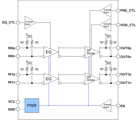
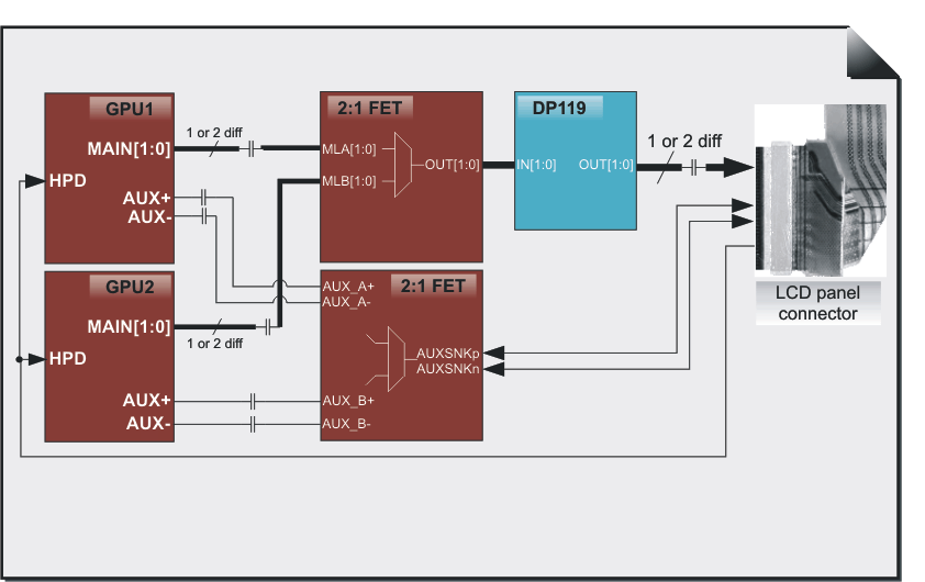 Figure 7. Typical Implementation Showing Two GPU Sources, a 2:1 FET Switch, and the DP119 as Signal Conditioner
9.3 Feature Description
9.3.1 Pre-Emphasis and VOD Output Swing Setings
The SN75DP119 allows configuring output pre-emphasis and output swing through the external control inputs. The following options are valid:
Table 1. Pre-Emphasis and VOD Output Swing Configuration
| PRE_CTL = LOW | PRE_CTL = VCC/2 (INPUT LEFT FLOATING) |
PRE_CTL = HIGH | |
|---|---|---|---|
| VOD_CTL = LOW | VOD = 300 mVPP; 2.5 dB pre-emphasis (lowest power consumption) |
VOD = 300 mVPP; 6 dB pre-emphasis |
VOD = 300 mVPP; 8.5 dB pre-emphasis |
| VOD_CTL = VCC/2
(input left floating) |
VOD = 400 mVPP; no pre-emphasis |
VOD = 400 mVPP; 3.5 dB pre-emphasis |
VOD = 400 mVPP; 5.5 dB pre-emphasis |
| VOD_CTL = HIGH | VOD = 600 mVPP; no pre-emphasis |
VOD = 600 mVPP; 2.5 dB pre-emphasis |
VOD = 800 mVPP, no pre-emphasis |
9.4 Device Functional Modes
9.4.1 Status Detect and Operating Modes Flow Diagram
The SN75DP119 switches between the power saving and the active modes in the following way:
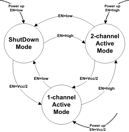 Figure 8. SN75DP119 Operational Modes Flow Chart
Table 2. Description of SN75DP119 Modes
| MODE | CHARACTERISTICS | CONDITIONS |
|---|---|---|
| ShutDown Mode | Least amount of power consumption (all circuitry turned off); outputs are high-impedance | EN is low |
| 2- channel Active Mode | Data transfer (normal operation); The device outputs OUTx represents the data received on the input INx. The input EQ and output pre-emphasis and output swing voltage level are controlled through the external control pins. | EN is high (both main link outputs enabled) |
| 1-channel Active Mode | Data transfer (normal operation); The device output OUT0 represents the data received on the input IN0. The 2nd channel (IN1 and OUT1) are disabled. The input EQ and output pre-emphasis and output swing voltage level are controlled through the external control pins. | EN is VCC/2 (only main link channel 0 enabled) |