SLLSE12A November 2009 – July 2014 SN75DP119
PRODUCTION DATA.
- 1 Features
- 2 Applications
- 3 Description
- 4 Revision History
- 5 Description (continued)
- 6 Pin Configuration and Functions
- 7 Specifications
- 8 Parameter Measurement Information
- 9 Detailed Description
- 10Application and Implementation
- 11Power Supply Recommendations
- 12Layout
- 13Device and Documentation Support
- 14Mechanical, Packaging, and Orderable Information
Package Options
Mechanical Data (Package|Pins)
Thermal pad, mechanical data (Package|Pins)
Orderable Information
10 Application and Implementation
10.1 Application Information
Figure 9 provides a simple schematic reference for the 14-pin package. In addition to this schematic sufficient VCC decoupling for the 3.3V power supply is necessary.
10.2 Typical Application
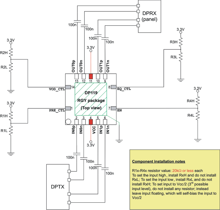 Figure 9. Simplified Schematic drawing
10.2.1 Design Requirements
For this design example, use the following as the input parameters.
Table 3. Design Parameters
| DESIGN PARAMETER | EXAMPLE VALUE |
|---|---|
| VCC | 3.3 V |
| Main Link Input Voltage | VID = 0.15 to 1.4 Vpp |
| Control Pin Max Voltage for Low | 0.5 V |
| Control Pin Voltage Range Mid | Min (VCC/2) - 0.3 V to Max of (VCC/2) + 0.3 V |
| Control Pin Min Voltage for High | Min VCC - 0.5 V |
| Main Link AC Decoupling Cap | 75 nF to 200 nF Recommend 100 nF |
10.2.2 Detailed Design Procedure
- Determine the output swing of the Graphic Processing Unit (GPU) .
- Determine the loss profile between the GPU and the LCD display connector.
- Determine the loss profile between the mother board LCD display connector and the DisplayPort receiver.
- Determine the DisplayPort receiver capabilities, acceptable VID along with its receive equalizer capability.
- Based upon this loss profile and signal swing determine optimal location for the SN75DP119, close to the connector, midway, or close to GPU.
- Use the typical application drawing, Figure 9, for information on using the AC coupling caps and control pin resistors.
- Set the DP119 Input equalizer appropriately to support the loss profile and signal swing for the link between the GPU and connector by using the EQ_CTL control pin.
- Set the DP119 VOD and Pre-emphasis level appropriately to support the Connector to DisplayPort receiver link by using the PRE_CTL and VOC_CTL control pins.
- The thermal pad must be connected to ground.
- Use a 1 µF and 0.1 µF decouple caps from VCC pins to Ground.
10.2.3 Application Curves
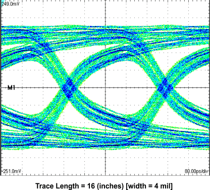
| DR = 2.7 Gbps | VOD = 400 mVpp | PRE = 0 dB |
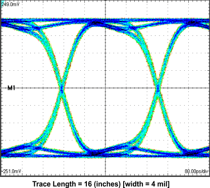
| DR = 2.7 Gbps | VOD = 400 mVpp | PRE = 0 dB |