SLOS921B December   2015  – September 2018 TAS5411-Q1

PRODUCTION DATA.  

  1. Features
  2. Applications
  3. Description
    1.     Device Images
      1.      Simplified Block Diagram
      2.      Efficiency
  4. Revision History
  5. Device Comparison Table
  6. Pin Configuration and Functions
    1.     Pin Functions
  7. Specifications
    1. 7.1 Absolute Maximum Ratings
    2. 7.2 ESD Ratings
    3. 7.3 Recommended Operating Conditions
    4. 7.4 Thermal Information
    5. 7.5 Electrical Characteristics
    6. 7.6 Timing Requirements for I2C Interface Signals
    7. 7.7 Typical Characteristics
  8. Parameter Measurement Information
  9. Detailed Description
    1. 9.1 Overview
    2. 9.2 Functional Block Diagram
    3. 9.3 Feature Description
      1. 9.3.1 Analog Audio Input and Preamplifier
      2. 9.3.2 Pulse-Width Modulator (PWM)
      3. 9.3.3 Gate Drive
      4. 9.3.4 Power FETs
      5. 9.3.5 Load Diagnostics
        1. 9.3.5.1 Load Diagnostics Sequence
        2. 9.3.5.2 Faults During Load Diagnostics
      6. 9.3.6 Protection and Monitoring
      7. 9.3.7 I2C Serial Communication Bus
        1. 9.3.7.1 I2C Bus Protocol
        2. 9.3.7.2 Random Write
        3. 9.3.7.3 Random Read
        4. 9.3.7.4 Sequential Read
    4. 9.4 Device Functional Modes
      1. 9.4.1 Hardware Control Pins
      2. 9.4.2 EMI Considerations
      3. 9.4.3 Operating Modes and Faults
    5. 9.5 Register Maps
  10. 10Application and Implementation
    1. 10.1 Application Information
    2. 10.2 Typical Application
      1. 10.2.1 Design Requirements
        1. 10.2.1.1 Amplifier Output Filtering
        2. 10.2.1.2 Amplifier Output Snubbers
        3. 10.2.1.3 Bootstrap Capacitors
        4. 10.2.1.4 Analog Audio Input Filter
      2. 10.2.2 Detailed Design Procedure
        1. 10.2.2.1 Unused Pin Connections
          1. 10.2.2.1.1 MUTE Pin
          2. 10.2.2.1.2 STANDBY Pin
          3. 10.2.2.1.3 I2C Pins (SDA and SCL)
          4. 10.2.2.1.4 Terminating Unused Outputs
          5. 10.2.2.1.5 Using a Single-Ended Audio Input
      3. 10.2.3 Application Curves
  11. 11Power Supply Recommendations
  12. 12Layout
    1. 12.1 Layout Guidelines
    2. 12.2 Layout Examples
      1. 12.2.1 Top Layer
      2. 12.2.2 Second Layer – Signal Layer
      3. 12.2.3 Third Layer – Power Layer
      4. 12.2.4 Bottom Layer – Ground Layer
  13. 13Device and Documentation Support
    1. 13.1 Device Support
      1. 13.1.1 Third-Party Products Disclaimer
    2. 13.2 Documentation Support
      1. 13.2.1 Related Documentation
    3. 13.3 Receiving Notification of Documentation Updates
    4. 13.4 Community Resources
    5. 13.5 Trademarks
    6. 13.6 Electrostatic Discharge Caution
    7. 13.7 Glossary
  14. 14Mechanical, Packaging, and Orderable Information

Package Options

Mechanical Data (Package|Pins)
Thermal pad, mechanical data (Package|Pins)
Orderable Information

Third Layer – Power Layer

There is no need for a power plane, but TI recommends a wide single PVDD trace to keep the switching noise to a minimum and provide enough current to the device. The wide trace provides a low-impedance path from the power source to the PVDD pin and from the GND pin to the source return. Suppression of switching noise (ripple voltage) on both the positive and return (ground) paths requires a low impedance.
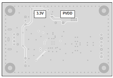
TAS5411-Q1 Layer3_SLOS814.pngFigure 20. Power Layer