SLVS638D January 2006 – June 2022
PRODUCTION DATA
- 1 Features
- 2 Applications
- 3 Description
- 4 Revision History
- 5 Pin Configuration and Functions
- 6 Specifications
- 7 Parameter Measurement Information
- 8 Detailed Description
- 9 Application and Implementation
- 10Power Supply Recommendations
- 11Layout
- 12Device and Documentation Support
- 13Mechanical, Packaging, and Orderable Information
Package Options
Mechanical Data (Package|Pins)
Thermal pad, mechanical data (Package|Pins)
- KTT|5
Orderable Information
9.1.2.8 Buck Regulator Design Procedure
| PROCEDURE (Fixed Output) | EXAMPLE (Fixed Output) |
|---|---|
Known: VOUT = 3.3 V, 5 V, 12 V, or 15 V VIN(Max) = Maximum input voltage ILOAD(Max) = Maximum load current | Known: VOUT = 5 V VIN(Max) = 20 V ILOAD(Max) = 1 A |
1. Inductor Selection (L1) | 1. Inductor Selection (L1) |
A. From Figure 9-2 through Figure 9-5, select the appropriate inductor code based on the intersection of VIN(Max) and ILOAD(Max). | A. From Figure 9-3 (TL2575-05), the intersection of 20-V line and 1-A line gives an inductor code of L330. |
B. The inductor chosen should be rated for operation at 52-kHz and have a current rating of at least 1.15 × ILOAD(Max) to allow for the ripple current. The actual peak current in L1 (in normal operation) can be calculated as follows: IL1(pk) = ILOAD(Max) + (VIN – VOUT) × ton / 2L1 Where ton = VOUT / VIN × (1 / fosc) | B. L330 → L1 = 330 μH Choose from: 34042 (Schott) PE-52627 (Pulse Engineering) RL1952 (Renco) |
2. Output Capacitor Selection (COUT) | 2. Output Capacitor Selection (COUT) |
A. The TL2575 control loop has a two-pole two-zero frequency response. The dominant pole-zero pair is established by COUT and L1. To meet stability requirements while maintaining an acceptable output ripple voltage (Vripple ≉ 0.01 × VOUT), the recommended range for a standard aluminum electrolytic COUT is between 100 μF and 470 μF. | A. COUT = 100-μF to 470-μF, standard aluminum electrolytic |
B. COUT should have a voltage rating of at least 1.5 × VOUT. But if a low output ripple voltage is desired, choose capacitors with a higher-voltage ratings than the minimum required, due to their typically lower ESRs. | B. Although a COUT rated at 8 V is sufficient for VOUT = 5 V, a higher-voltage capacitor is chosen for its typically lower ESR (and hence lower output ripple voltage) → Capacitor voltage rating = 20 V. |
3. Catch Diode Selection (D1) (see Table 9-1) | 3. Catch Diode Selection (D1) (see Table 9-1) |
A. In normal operation, the catch diode requires a current rating of at least 1.2 × ILOAD(Max). For the most robust design, D1 should be rated to handle a current equal to the TL2575 maximum switch peak current; this represents the worst-case scenario of a continuous short at VOUT. | A. Pick a diode with 3-A rating. |
B. The diode requires a reverse voltage rating of at least 1.25 × VIN(Max). | B. Pick 30-V rated Schottky diode (1N5821, MBR330, 31QD03, or SR303) or 100-V rated Fast Recovery diode (31DF1, MURD310, or HER302). |
4. Input Capacitor (CIN) An aluminum electrolytic or tantalum capacitor is needed for input bypassing. Locate CIN as close to the VIN and GND pins as possible. | 4. Input Capacitor (CIN) CIN = 100 μF, 25 V, aluminum electrolytic |
| PROCEDURE (Adjustable Output) | EXAMPLE (Adjustable Output) |
|---|---|
Known: VOUT(Nom) VIN(Max) = Maximum input voltage ILOAD(Max) = Maximum load current | Known: VOUT = 10 V VIN(Max) = 25 V ILOAD(Max) = 1 A |
1. Programming Output Voltage (Selecting R1 and R2) Referring to Figure 6-2, VOUT is defined by: 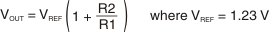 Choose a value for R1 between 1 kΩ and 5 kΩ (use 1% metal-film resistors for best temperature coefficient and stability over time). 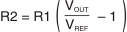 | 1. Programming Output Voltage (Selecting R1 and R2) Select R1 = 1 kΩ R2 = 1 (10 / 1.23 – 1) = 7.13 kΩ Select R2 = 7.15 kΩ (closest 1% value) |
2. Inductor Selection (L1) | 2. Inductor Selection (L1) |
A. Calculate the "set" volts-second (E × T) across L1: E × T = (VIN – VOUT) × ton E × T = (VIN – VOUT) × (VOUT / VIN) × {1000 / fosc(in kHz)} [V × μs] Note: NOTE: Along with ILOAD, the "set" volts-second (E × T) constant establishes the minimum energy storage requirement for the inductor. | A. Calculate the "set" volts-second (E × T) across L1: E × T = (25 – 10) × (10 / 25) × (1000 / 52) [V × μs] E × T = 115 V × μs |
B. Using Figure 9-6, select the appropriate inductor code based on the intersection of E × T value and ILOAD(Max). | B. Using Figure 9-6, the intersection of 115 V • μs and 1 A corresponds to an inductor code of H470. |
C. The inductor chosen should be rated for operation at 52-kHz and have a current rating of at least 1.15 x ILOAD(Max) to allow for the ripple current. The actual peak current in L1 (in normal operation) can be calculated as follows: IL1(pk) = ILOAD(Max) + (VIN – VOUT) × ton / 2L1 Where ton = VOUT / VIN × (1 / fosc) | C. H470 → L1 = 470 μH Choose from: 34048 (Schott) PE-53118 (Pulse Engineering) RL1961 (Renco) |
3. Output Capacitor Selection (COUT) | 3. Output Capacitor Selection (COUT) |
A. The TL2575 control loop has a two-pole two-zero frequency response. The dominant pole-zero pair is established by COUT and L1. To meet stability requirements, COUT must meet the following requirement:  However, COUT may need to be several times larger than the calculated value above in order to achieve an acceptable output ripple voltage of ~0.01 × VOUT. | A. COUT ≥ 7785 × 25 / (10 × 470) [μF] COUT ≥ 41.4 μF To obtain an acceptable output voltage ripple → COUT = 220 μF electrolytic |
B. COUT should have a voltage rating of at least 1.5 × VOUT. But if a low output ripple voltage is desired, choose capacitors with a higher voltage ratings than the minimum required due to their typically lower ESRs. | |
4. Catch Diode Selection (D1) (see Table 9-1) | 4. Catch Diode Selection (D1) (see Table 9-1) |
A. In normal operation, the catch diode requires a current rating of at least 1.2 × ILOAD(Max). For the most robust design, D1 should be rated for a current equal to the TL2575 maximum switch peak current; this represents the worst-case scenario of a continuous short at VOUT. | A. Pick a diode with a 3-A rating. |
B. The diode requires a reverse voltage rating of at least 1.25 × VIN(Max). | B. Pick a 40-V rated Schottky diode (1N5822, MBR340, 31QD04, or SR304) or 100-V rated Fast Recovery diode (31DF1, MURD310, or HER302) |
5. Input Capacitor (CIN) An aluminum electrolytic or tantalum capacitor is needed for input bypassing. Locate CIN as close to VIN and GND pins as possible. | 5. Input Capacitor (CIN) CIN = 100 μF, 35 V, aluminum electrolytic |
| VR | SCHOTTKY | FAST RECOVERY | ||
|---|---|---|---|---|
| 1A | 3A | 1A | 3A | |
| 20 V | 1N5817 MBR120P SR102 | 1N5820 MBR320 SR302 | The following diodes are all rated to 100 V: 11DF1 MUR110 HER102 | The following diodes are all rated to 100 V: 31DF1 MURD310 HER302 |
| 30 V | 1N5818 MBR130P 11DQ03 SR103 | 1N5821 MBR330 31DQ03 SR303 | ||
| 40 V | 1N5819 MBR140P 11DQ04 SR104 | IN5822 MBR340 31DQ04 SR304 | ||
| 50 V | MBR150 11DQ05 SR105 | MBR350 31DQ05 SR305 | ||
| 60 V | MBR160 11DQ06 SR106 | MBR360 31DQ06 SR306 | ||