SLVS638D January   2006  – June 2022

PRODUCTION DATA  

  1. Features
  2. Applications
  3. Description
  4. Revision History
  5. Pin Configuration and Functions
  6. Specifications
    1. 6.1 Absolute Maximum Ratings
    2. 6.2 ESD Ratings
    3. 6.3 Recommended Operating Conditions
    4. 6.4 Thermal Information
    5. 6.5 Electrical Characteristics — TL2575
    6. 6.6 Electrical Characteristics — TL2575HV
    7. 6.7 Typical Characteristics
  7. Parameter Measurement Information
    1. 7.1 Test Circuits
  8. Detailed Description
    1. 8.1 Overview
    2. 8.2 Functional Block Diagram
    3. 8.3 Feature Description
      1. 8.3.1 Feedback Connection
      2. 8.3.2 ON/OFF Input
    4. 8.4 Device Functional Modes
      1. 8.4.1 Standby Mode
  9. Application and Implementation
    1. 9.1 Typical Application
      1. 9.1.1 Design Requirements
      2. 9.1.2 Detailed Design Procedure
        1. 9.1.2.1 Input Capacitor (CIN)
        2. 9.1.2.2 Output Capacitor (COUT)
        3. 9.1.2.3 Catch Diode
        4. 9.1.2.4 Inductor
        5. 9.1.2.5 Output Voltage Ripple and Transients
        6. 9.1.2.6 Grounding
        7. 9.1.2.7 Reverse Current Considerations
        8. 9.1.2.8 Buck Regulator Design Procedure
        9. 9.1.2.9 Inductor Selection Guide
      3. 9.1.3 Application Curves
  10. 10Power Supply Recommendations
  11. 11Layout
    1. 11.1 Layout Guidelines
    2. 11.2 Layout Example
  12. 12Device and Documentation Support
    1. 12.1 Receiving Notification of Documentation Updates
    2. 12.2 Support Resources
    3. 12.3 Trademarks
    4. 12.4 Electrostatic Discharge Caution
    5. 12.5 Glossary
  13. 13Mechanical, Packaging, and Orderable Information
    1. 13.1 Package Option Addendum

Package Options

Mechanical Data (Package|Pins)
Thermal pad, mechanical data (Package|Pins)
Orderable Information

Description

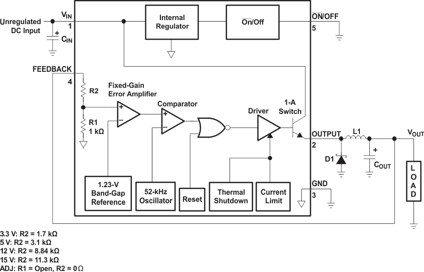
The TL2575 and TL2575HV devices provide all the active functions needed for a step-down (buck) switching regulator in an integrated circuit. They require four to six external components for operation. They accept a wide input-voltage range of up to 60 V (TL2575-HV) and are available in fixed output voltages of 3.3 V, 5 V, 12 V, 15 V, or an adjustable-output version. The TL2575 and TL2575HV devices have an integrated switch capable of delivering 1 A of load current, with excellent line and load regulation. The device also offers internal frequency compensation, a fixed-frequency oscillator, cycle-by-cycle current limiting, and thermal shutdown. In addition, a manual shutdown is available through the external ON/OFF pin.

Device Information
PART NUMBER PACKAGE(1) BODY SIZE (NOM)
TL2575, TL2575HV PDIP (16) 19.31 mm × 6.35 mm
TO-263 (5) 10.16 mm × 8.93 mm
TO-220 (5) 10.16 mm × 8.82 mm
For all available packages, see the orderable addendum at the end of the data sheet.
GUID-E62F7AB8-2F64-45F5-91B0-9447BD0E8BDF-low.gif
Pin numbers are for the KTT (TO-263) package.
Functional Block Diagram