SBVS114B July 2008 – January 2015 TLC5947
PRODUCTION DATA.
- 1 Features
- 2 Applications
- 3 Description
- 4 Revision History
- 5 Pin Configuration and Functions
- 6 Specifications
- 7 Parameter Measurement Information
- 8 Detailed Description
- 9 Application and Implementation
- 10Power Supply Recommendations
- 11Layout
- 12Device and Documentation Support
- 13Mechanical, Packaging, and Orderable Information
Package Options
Mechanical Data (Package|Pins)
Thermal pad, mechanical data (Package|Pins)
Orderable Information
8 Detailed Description
8.1 Overview
The TLC5947 is a 24-channel, constant-current sink driver. Each channel has an individually-adjustable, 4096-step, PWM grayscale (GS) brightness control. The GS data is input through a serial interface port.
The TLC5947 has a 30-mA current capability. The maximum current value of all channels is determined by an external resistor.
The TLC5947 can work without external CLK signals because the device is integrated with a 4-MHz internal oscillator.
The device has a thermal shutdown (TSD) function that turns off all output drivers at over temperature conditions. All of the output drivers automatically restart when the temperature returns to normal conditions.
8.2 Functional Block Diagram
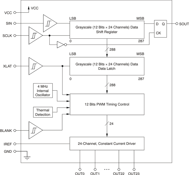
8.3 Feature Description
8.3.1 Grayscale (GS) Control Function
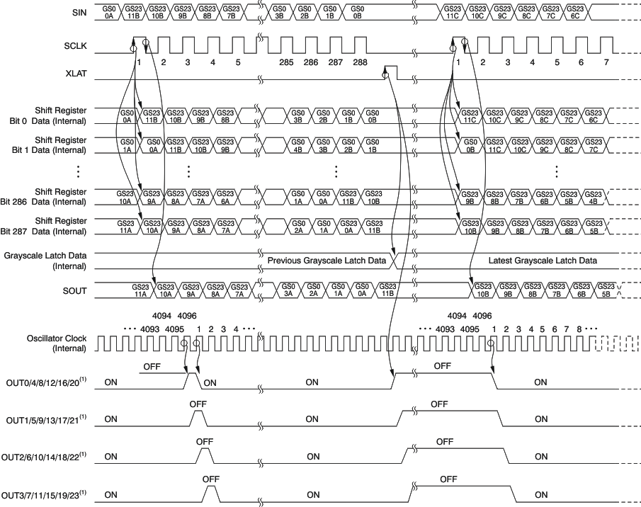
Each constant-current sink output OUT0–OUT23 (OUTn) turns on (starts to sink constant current) at the fifth rising edge of the grayscale internal oscillator clock after the BLANK signal transitions from high to low if the grayscale data latched into the grayscale data latch are not zero. After turn-on, the number of rising edges of the internal oscillator is counted by the 12-bit grayscale counter. Each OUTn output is turned off once its corresponding grayscale data values equal the grayscale counter or the counter reaches 4096d (FFFh). The PWM control operation is repeated as long as BLANK is low. OUTn is not turned on when BLANK is high. The timing is shown in Figure 18. All outputs are turned off at the XLAT rising edge. After that, each output is controlled again from the first clock of the internal oscillator for the next display period, based on the latest grayscale data.
When the IC is powered on, the data in the grayscale data shift register and latch are not set to default values. Therefore, grayscale data must be written to the GS latch before turning on the constant-current output. BLANK should be at a high level when powered on to keep the outputs off until valid grayscale data are written to the latch. This avoids the LED being randomly illuminated immediately after power-up. If having the outputs turn on at power-up is not a problem for the application, then BLANK does not need to be held high. The grayscale functions can be controlled directly by grayscale data writing, even though BLANK is connected to GND.
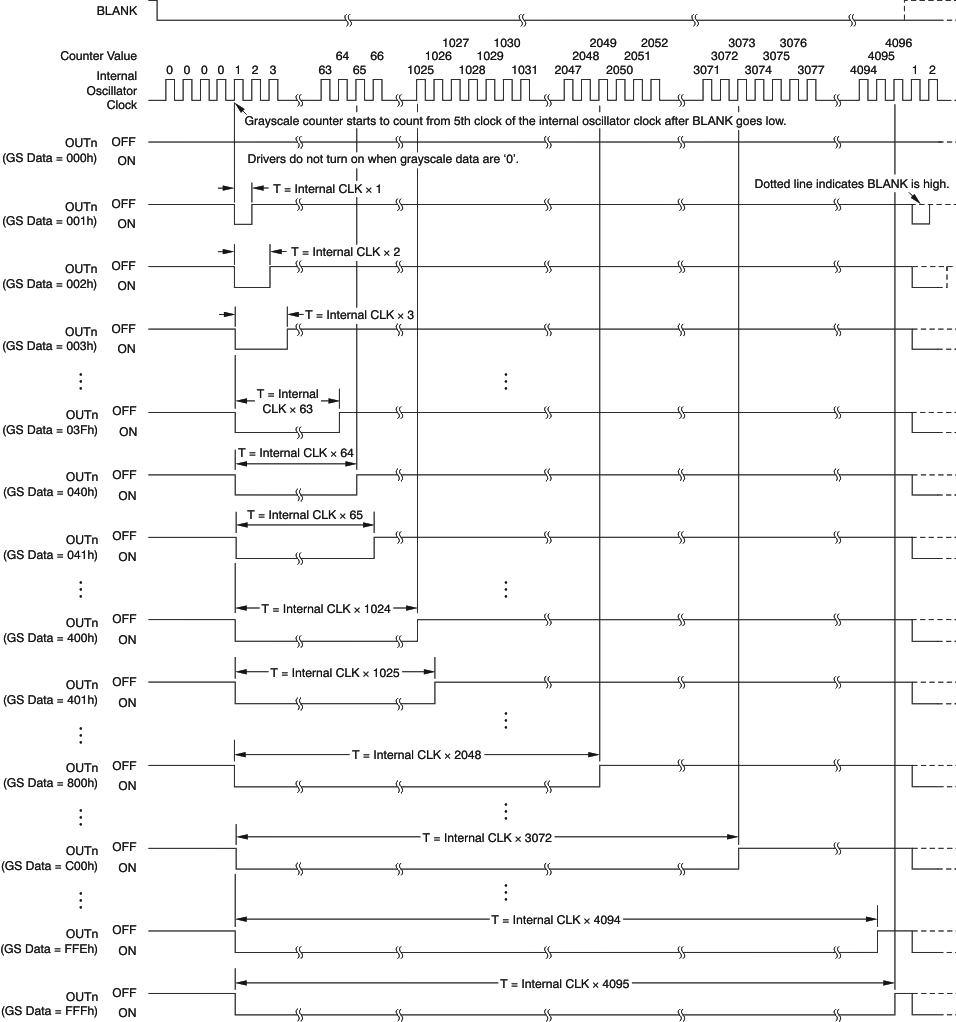 Figure 18. PWM Operation
8.3.2 Auto Display Repeat Function
This function can repeat the total display period without any timing control signal, as shown in Figure 19.
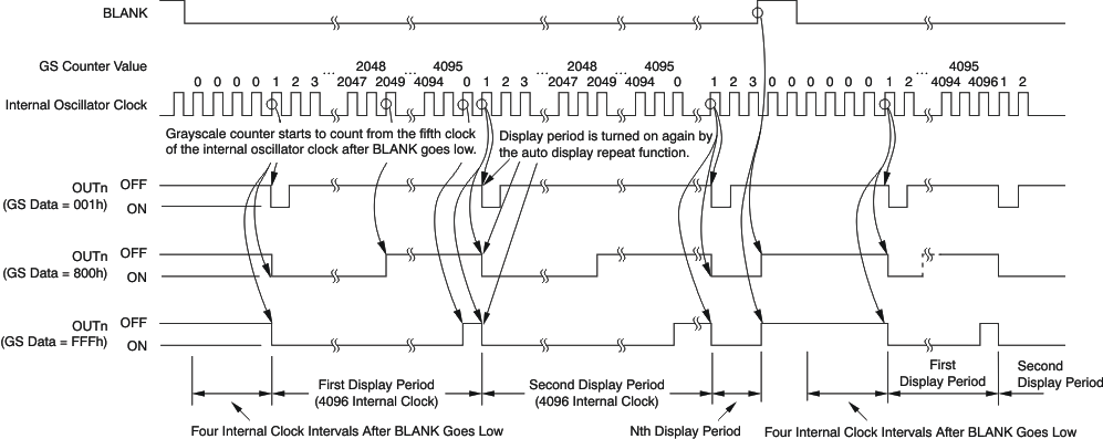 Figure 19. Auto Display Repeat Operation
8.3.3 Thermal Shutdown (TSD)
The thermal shutdown (TSD) function turns off all constant-current outputs immediately when the IC junction temperature exceeds the high temperature threshold (T(TEF) = +162° C, typ). The outputs will remain disabled as long as the over-temperature condition exists. The outputs are turned on again at the first clock after the IC junction temperature falls below the temperature of T(TEF) – T(HYS). Figure 20 shows the TSD operation.
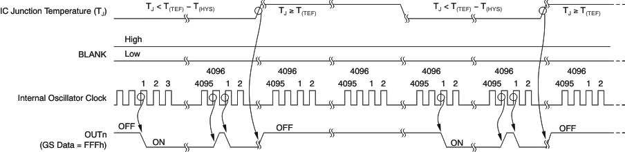 Figure 20. TSD Operation
8.3.4 Noise Reduction
Large surge currents may flow through the IC and the board on which the device is mounted if all 24 LED channels turn on simultaneously at the start of each grayscale cycle. These large current surges could introduce detrimental noise and electromagnetic interference (EMI) into other circuits. The TLC5947 turns on the LED channels in a series delay, to provide a current soft-start feature. The output current sinks are grouped into four groups of six channels each. The first group is OUT0, 4, 8, 12, 16, 20; the second group is OUT1, 5, 9, 13, 17, 21; the third group is OUT2, 6, 10, 14, 18, 22; and the fourth group is OUT3, 7, 11, 15, 19, 23. Each group turns on sequentially with a small delay between groups; see Figure 3. Both turn-on and turn-off are delayed.
8.4 Programming
8.4.1 Register Configuration
The TLC5947 has a grayscale (GS) data shift register and data latch. Both the GS data shift register and latch are 288 bits long and are used to set the PWM timing for the constant-current driver. Table 1 shows the on duty cycle for each GS data. Figure 21 shows the shift register and data latch configuration. The data at the SIN pin are shifted to the LSB of the shift register at the rising edge of the SCLK pin; SOUT data are shifted out on the falling edge of SCLK. The timing diagram for data writing is shown in Figure 22. The driver on duty is controlled by the data in the GS data latch.
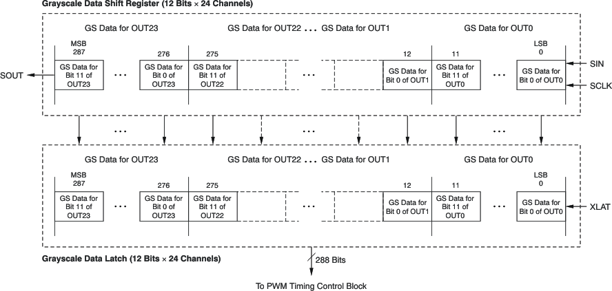 Figure 21. Grayscale Data Shift Register and Latch Configuration
Table 1. GS Data versus On Duty
| GS DATA (Binary) |
GS DATA (Decimal) |
GS DATA (Hex) |
DUTY OF DRIVER TURN-ON TIME (%) |
|---|---|---|---|
| 0000 0000 0000 | 0 | 000 | 0.00 |
| 0000 0000 0001 | 1 | 001 | 0.02 |
| 0000 0000 0010 | 2 | 002 | 0.05 |
| 0000 0000 0011 | 3 | 003 | 0.07 |
| — | — | — | — |
| 0111 1111 1111 | 2047 | 7FF | 49.98 |
| 1000 0000 0000 | 2048 | 800 | 50.00 |
| 1000 0000 0001 | 2049 | 801 | 50.02 |
| — | — | — | — |
| 1111 1111 1101 | 4093 | FFD | 99.93 |
| 1111 1111 1110 | 4094 | FFE | 99.95 |
| 1111 1111 1111 | 4095 | FFF | 99.98 |
GS data are transferred from the shift register to the latch by the rising edge of XLAT. When powered up, the data in the grayscale shift register and data latch are not set to default values. Therefore, grayscale data must be written to the GS latch before turning on the constant-current output. BLANK should be at a high level when powered on to avoid falsely turning on the constant-current outputs due to random values in the latch at power-up. All of the constant-current outputs are forced off when BLANK is high. However, if the random values turning on at power-up is not a concern in the application, BLANK can be at any level. GS can be controlled correctly with the grayscale data writing functions, even if BLANK is connected to GND. Equation 1 determines each output on duty.

where
- GSn = the programmed grayscale value for OUTn (GSn = 0 to 4095)
NOINDENT:
GS data = FFFh.