SBVS114B July 2008 – January 2015 TLC5947
PRODUCTION DATA.
- 1 Features
- 2 Applications
- 3 Description
- 4 Revision History
- 5 Pin Configuration and Functions
- 6 Specifications
- 7 Parameter Measurement Information
- 8 Detailed Description
- 9 Application and Implementation
- 10Power Supply Recommendations
- 11Layout
- 12Device and Documentation Support
- 13Mechanical, Packaging, and Orderable Information
Package Options
Mechanical Data (Package|Pins)
Thermal pad, mechanical data (Package|Pins)
Orderable Information
6 Specifications
6.1 Absolute Maximum Ratings
Over operating free-air temperature range, unless otherwise noted.(1)(2)| MIN | MAX | UNIT | |||
|---|---|---|---|---|---|
| VCC | Supply voltage: VCC | –0.3 | 6.0 | V | |
| IO | Output current (dc) | OUT0 to OUT23 | 38 | mA | |
| VI | Input voltage | SIN, SCLK, XLAT, BLANK | –0.3 | VCC + 0.3 | V |
| VO | Output voltage | SOUT | –0.3 | VCC + 0.3 | V |
| OUT0 to OUT23 | –0.3 | 33 | V | ||
| TJ(MAX) | Operating junction temperature | 150 | °C | ||
| Tstg | Storage temperature | –55 | 150 | °C | |
(1) Stresses beyond those listed under Absolute Maximum Ratings may cause permanent damage to the device. These are stress ratings only, which do not imply functional operation of the device at these or any other conditions beyond those indicated under Recommended Operating Conditions. Exposure to absolute-maximum-rated conditions for extended periods may affect device reliability.
(2) All voltage values are with respect to network ground terminal.
6.2 ESD Ratings
| VALUE | UNIT | ||||
|---|---|---|---|---|---|
| V(ESD) | Electrostatic discharge | Human body model (HBM), per ANSI/ESDA/JEDEC JS-001, all pins(1) | ±2500 | V | |
| Charged device model (CDM), per JEDEC specification JESD22-C101, all pins(2) | ±500 | ||||
(1) JEDEC document JEP155 states that 500-V HBM allows safe manufacturing with a standard ESD control process.
(2) JEDEC document JEP157 states that 250-V CDM allows safe manufacturing with a standard ESD control process.
6.3 Recommended Operating Conditions
At TA= –40°C to 85°C, unless otherwise noted.| MIN | NOM | MAX | UNIT | |||
|---|---|---|---|---|---|---|
| DC CHARACTERISTICS: VCC = 3 V to 5.5 V | ||||||
| VCC | Supply voltage | 3.0 | 5.5 | V | ||
| VO | Voltage applied to output OUT0 to OUT23 | 30 | V | |||
| VIH | High-level input voltage | 0.7 × VCC | VCC | V | ||
| VIL | Low-level input voltage | GND | 0.3 × VCC | V | ||
| IOH | High-level output current SOUT | –3 | mA | |||
| IOL | Low-level output current SOUT | 3 | mA | |||
| IOLC | Constant output sink current OUT0 to OUT23 | 2 | 30 | mA | ||
| TA | Operating free-air temperature range | –40 | 85 | °C | ||
| TJ | Operating junction temperature | –40 | 125 | °C | ||
| AC CHARACTERISTICS: VCC = 3 V to 5.5 V | ||||||
| fSCLK | Data shift clock frequency | SCLK, Standalone operation | 30 | MHz | ||
| SCLK, Duty 50%, cascade operation | 15 | MHz | ||||
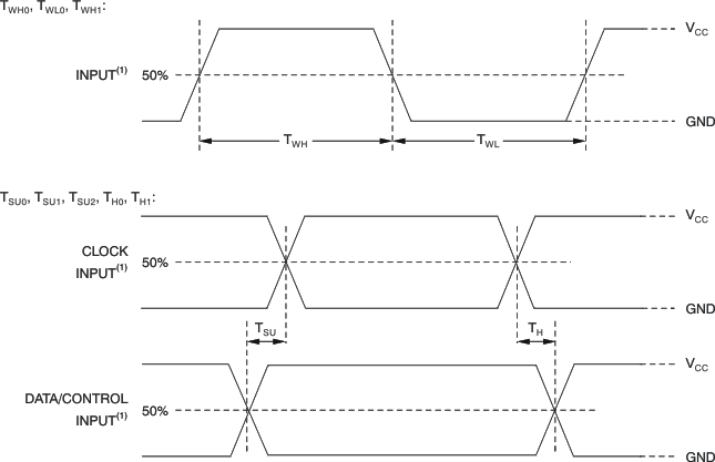
| TWH0 | Pulse duration | SCLK = High-level pulse width | 12 | ns | ||
| TWL0 | SCLK = Low-level pulse width | 10 | ns | |||
| TWH1 | XLAT, BLANK High-level pulse width | 30 | ns | |||
| TSU0 | Setup time | SIN–SCLK↑ | 5 | ns | ||
| TSU1 | XLAT↑–SCLK↑ | 100 | ns | |||
| TSU2 | XLAT↑–BLANK↓ | 30 | ns | |||
| TH0 | Hold time | SIN–SCLK↑ | 3 | ns | ||
| TH1 | XLAT↑–SCLK↑ | 10 | ns | |||
6.4 Thermal Information
| THERMAL METRIC(1) | TLC5947 | UNIT | |
|---|---|---|---|
| DAP | |||
| 32 PINS | |||
| RθJA | Junction-to-ambient thermal resistance | 32.8 | °C/W |
| RθJC(top) | Junction-to-case (top) thermal resistance | 17.1 | |
| RθJB | Junction-to-board thermal resistance | 17.9 | |
| ψJT | Junction-to-top characterization parameter | 0.4 | |
| ψJB | Junction-to-board characterization parameter | 17.8 | |
| RθJC(bot) | Junction-to-case (bottom) thermal resistance | 1.3 | |
(1) For more information about traditional and new thermal metrics, see the IC Package Thermal Metrics application report, SPRA953.
6.5 Dissipation Ratings
| PACKAGE | OPERATING FACTOR ABOVE TA = 25°C | TA < 25°C POWER RATING |
TA = 70°C POWER RATING |
TA = 85°C POWER RATING |
|---|---|---|---|---|
| HTSSOP-32 with PowerPAD™ soldered(1) |
42.54 mW/°C | 5318 mW | 3403 mW | 2765 mW |
| HTSSOP-32 with PowerPAD not soldered(2) |
22.56 mW/°C | 2820 mW | 1805 mW | 1466 mW |
| QFN-32(3) | 27.86 mW/°C | 3482 mW | 2228 mW | 1811 mW |
(1) With PowerPAD soldered onto copper area on printed circuit board (PCB); 2 oz. copper. For more information, see SLMA002.
(2) With PowerPAD not soldered onto copper area on PCB.
(3) The package thermal impedance is calculated in accordance with JESD51-5.
6.6 Electrical Characteristics
At VCC = 3.0 V to 5.5 V and TA = –40°C to 85°C. Typical values at VCC = 3.3 V and TA = 25°C, unless otherwise noted.| PARAMETER | TEST CONDITIONS | MIN | TYP | MAX | UNIT | |
|---|---|---|---|---|---|---|
| VOH | High-level output voltage | IOH = –3 mA at SOUT | VCC – 0.4 | VCC | V | |
| VOL | Low-level output voltage | IOL = 3 mA at SOUT | 0.4 | V | ||
| IIN | Input current | VIN = VCC or GND at SIN, XLAT, and BLANK | –1 | 1 | μA | |
| ICC1 | Supply current (VCC) | SIN/SCLK/XLAT = low, BLANK = high, VOUTn = 1 V, RIREF = 24 kΩ | 0.5 | 3 | mA | |
| ICC2 | SIN/SCLK/XLAT = low, BLANK = high, VOUTn = 1 V, RIREF = 3.3 kΩ | 1 | 6 | mA | ||
| ICC3 | SIN/SCLK/XLAT = low, BLANK = low, VOUTn = 1 V, RIREF = 3.3 kΩ, GSn = FFFh | 15 | 45 | mA | ||
| ICC4 | SIN/SCLK/XLAT = low, BLANK = low, VOUTn = 1 V, RIREF = 1.6 kΩ, GSn = FFFh | 30 | 90 | mA | ||
| IOLC | Constant output current | All OUTn = ON, VOUTn = 1 V, VOUTfix = 1 V, RIREF = 1.6 kΩ |
27.7 | 30.75 | 33.8 | mA |
| IOLK | Output leakage current | BLANK = high, VOUTn = 30 V, RIREF = 1.6 kΩ, At OUT0 to OUT23 |
0.1 | μA | ||
| ΔIOLC | Constant-current error (channel-to-channel)(1) |
All OUTn = ON, VOUTn = 1 V, VOUTfix = 1 V, RIREF = 1.6 kΩ, At OUT0 to OUT23 |
–4% | ±2% | 4% | |
| ΔIOLC1 | Constant-current error (device-to-device)(2) |
All OUTn = ON, VOUTn = 1 V, VOUTfix = 1 V, RIREF = 1.6 kΩ |
–7% | ±2% | 7% | |
| ΔIOLC2 | Line regulation(3) | All OUTn = ON, VOUTn = 1 V, VOUTfix = 1 V, RIREF = 1.6 kΩ, At OUT0 to OUT23 |
±1 | ±3 | %/V | |
| ΔIOLC3 | Load regulation(4) | All OUTn = ON, VOUTn = 1 V to 3 V, VOUTfix = 1 V, RIREF = 1.6 kΩ, At OUT0 to OUT23 | ±2 | ±6 | %/V | |
| TDOWN | Thermal shutdown threshold | Junction temperature(5) | 150 | 162 | 175 | °C |
| THYS | Thermal error hysteresis | Junction temperature(5) | 5 | 10 | 20 | °C |
| VIREF | Reference voltage output | RIREF = 1.6 kΩ | 1.16 | 1.20 | 1.24 | V |
(1) The deviation of each output from the average of OUT0–OUT23 constant-current. Deviation is calculated by the formula:
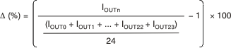 .
.
.(2) The deviation of the OUT0–OUT23 constant-current average from the ideal constant-current value. Deviation is calculated by the following formula:
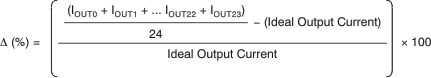 Ideal current is calculated by the formula:
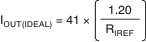
Ideal current is calculated by the formula:
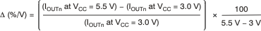
(3) Line regulation is calculated by this equation:
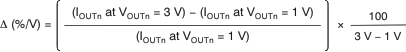
(4) Load regulation is calculated by the equation:
(5) Not tested. Specified by design.
6.7 Switching Characteristics
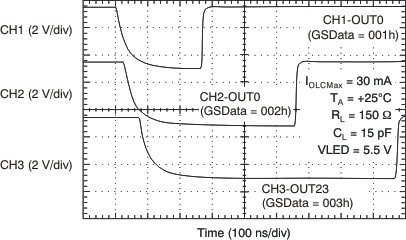
At VCC = 3.0 V to 5.5 V, TA = –40°C to 85°C, CL = 15 pF, RL = 150 Ω, RIREF = 1.6 kΩ, and VLED = 5.5 V. Typical values at VCC = 3.3 V and TA = 25°C, unless otherwise noted.| PARAMETER | TEST CONDITIONS | MIN | TYP | MAX | UNIT | |
|---|---|---|---|---|---|---|
| tR0 | Rise time | SOUT | 10 | 15 | ns | |
| tR1 | OUTn | 15 | 40 | ns | ||
| tF0 | Fall time | SOUT | 10 | 15 | ns | |
| tF1 | OUTn | 100 | 300 | ns | ||
| fOSC | Internal oscillator frequency | 2.4 | 4 | 5.6 | MHz | |
| tD0 | Propagation delay time | SCLK↓ to SOUT | 15 | 25 | ns | |
| tD1 | BLANK↑ to OUT0 sink current off | 20 | 40 | ns | ||
| tD2 | OUT0 current on to OUT1/5/9/13/17/21 current on | 15 | 24 | 33 | ns | |
| tD3 | OUT0 current on to OUT2/6/10/14/18/22 current on | 30 | 48 | 66 | ns | |
| tD4 | OUT0 current on to OUT3/7/11/15/19/23 current on | 45 | 72 | 99 | ns | |
1. Input pulse rise and fall time is 1 ns to 3 ns.
Figure 1. Input Timing
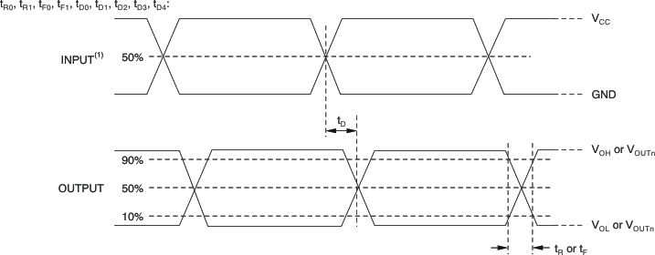
1. Input pulse rise and fall time is 1 ns to 3 ns.
Figure 2. Output Timing
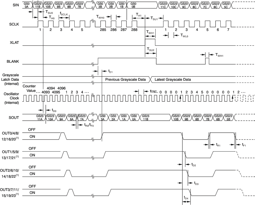
1. GS data = FFFh.
Figure 3. Grayscale Data Write and OUTn Operation Timing
6.8 Typical Characteristics
At VCC = 3.3 V and TA = 25°C, unless otherwise noted.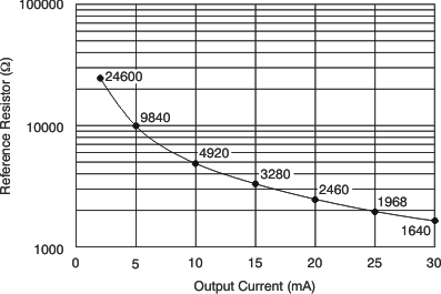 Figure 4. Reference Resistor vs Output Current
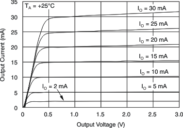 Figure 6. Output Current vs Output Voltage
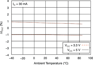 Figure 8. ΔIOLC vs Ambient Temperature
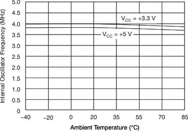 Figure 10. Internal Oscillator Frequency vs Ambient Temperature
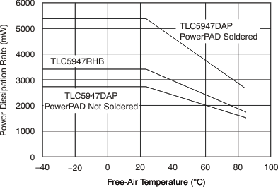 Figure 5. Power Dissipation Rate vs Free-Air Temperature
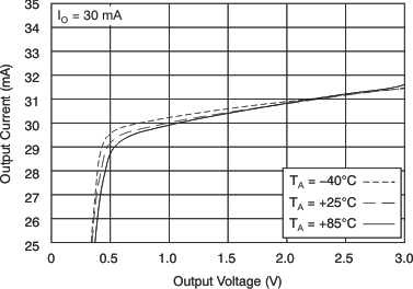 Figure 7. Output Current vs Output Voltage
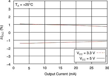 Figure 9. ΔIOLC vs Output Current