SBVS114B July 2008 – January 2015 TLC5947
PRODUCTION DATA.
- 1 Features
- 2 Applications
- 3 Description
- 4 Revision History
- 5 Pin Configuration and Functions
- 6 Specifications
- 7 Parameter Measurement Information
- 8 Detailed Description
- 9 Application and Implementation
- 10Power Supply Recommendations
- 11Layout
- 12Device and Documentation Support
- 13Mechanical, Packaging, and Orderable Information
Package Options
Mechanical Data (Package|Pins)
Thermal pad, mechanical data (Package|Pins)
Orderable Information
5 Pin Configuration and Functions
32-PINS
DAP PACKAGE
(TOP VIEW)
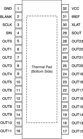
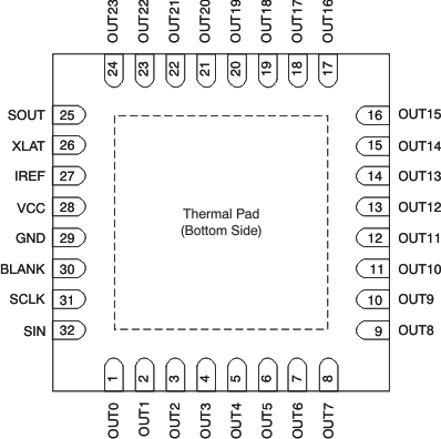
Pin Functions
| PIN | I/O | DESCRIPTION | ||
|---|---|---|---|---|
| NAME | RHB NO. | DAP NO. | ||
| BLANK | 30 | 2 | I | Blank (all constant-current outputs off). When BLANK is high, all constant-current outputs (OUT0 through OUT23) are forced off, the grayscale PWM timing controller initializes, and the grayscale counter resets to '0'. When BLANK is low, all constant-current outputs are controlled by the grayscale PWM timing controller. |
| GND | 29 | 1 | — | Power ground |
| IREF | 27 | 31 | I/O | This pin sets the constant-current value. OUT0 through OUT23 constant sink current is set to the desired value by connecting an external resistor between IREF and GND. |
| OUT0 | 1 | 5 | O | Constant-current output. Multiple outputs can be tied together to increase the constant-current capability. Different voltages can be applied to each output. |
| OUT1 | 2 | 6 | O | Constant-current output |
| OUT2 | 3 | 7 | O | Constant-current output |
| OUT3 | 4 | 8 | O | Constant-current output |
| OUT4 | 5 | 9 | O | Constant-current output |
| OUT5 | 6 | 10 | O | Constant-current output |
| OUT6 | 7 | 11 | O | Constant-current output |
| OUT7 | 8 | 12 | O | Constant-current output |
| OUT8 | 9 | 13 | O | Constant-current output |
| OUT9 | 10 | 14 | O | Constant-current output |
| OUT10 | 11 | 15 | O | Constant-current output |
| OUT11 | 12 | 16 | O | Constant-current output |
| OUT12 | 13 | 17 | O | Constant-current output |
| OUT13 | 14 | 18 | O | Constant-current output |
| OUT14 | 15 | 19 | O | Constant-current output |
| OUT15 | 16 | 20 | O | Constant-current output |
| OUT16 | 17 | 21 | O | Constant-current output |
| OUT17 | 18 | 22 | O | Constant-current output |
| OUT18 | 19 | 23 | O | Constant-current output |
| OUT19 | 20 | 24 | O | Constant-current output |
| OUT20 | 21 | 25 | O | Constant-current output |
| OUT21 | 22 | 26 | O | Constant-current output |
| OUT22 | 23 | 27 | O | Constant-current output |
| OUT23 | 24 | 28 | O | Constant-current output |
| SCLK | 31 | 3 | I | Serial data shift clock. Schmitt buffer input. Data present on the SIN pin are shifted into the shift register with the rising edge of the SCLK pin. Data are shifted to the MSB side by 1-bit synchronizing of the rising edge of SCLK. The MSB data appears on SOUT at the falling edge of SCLK. A rising edge on the SCLK input is allowed 100 ns after an XLAT rising edge. |
| SIN | 32 | 4 | I | Serial input for grayscale data |
| SOUT | 25 | 29 | O | Serial data output. This output is connected to the shift register placed after the MSB of the grayscale shift register. Therefore, the MSB data of the grayscale shift register appears at the falling edge of SCLK. This function reduces the data shifting errors caused by small timing margins between SIN and SCLK. |
| VCC | 28 | 32 | — | Power-supply voltage |
| XLAT | 26 | 30 | I | The data in the grayscale shift register are moved to the grayscale data latch with a low-to-high transition on this pin. When the XLAT rising edge is input, all constant-current outputs are forced off until the next grayscale display period. The grayscale counter is not reset to zero with a rising edge of XLAT. |