SLIS149 June 2014 TPL0102-EP
PRODUCTION DATA.
- 1 Features
- 2 Applications
- 3 Description
- 4 Functional Block Diagram
- 5 Revision History
- 6 Pin Configuration and Functions
- 7 Specifications
-
8 Detailed Description
- 8.1 Overview
- 8.2 Functional Block Diagram
- 8.3 Feature Description
- 8.4 Device Functional Modes
- 8.5
Register Maps
- 8.5.1 Slave Address
- 8.5.2 TPL0102-EP Register Maps
- 8.5.3 IVRA (Initial Value Register for Potentiometer A)
- 8.5.4 WRA (Wiper Resistance Register for Potentiometer A)
- 8.5.5 IVRB (Initial Value Register for Potentiometer B)
- 8.5.6 WRB (Wiper Resistance Register for Potentiometer B)
- 8.5.7 ACR (Access Control Register)
- 9 Application and Implementation
- 10Layout
- 11Device and Documentation Support
- 12Mechanical, Packaging, and Orderable Information
Package Options
Mechanical Data (Package|Pins)
- PW|14
Thermal pad, mechanical data (Package|Pins)
Orderable Information
6 Pin Configuration and Functions
TSSOP – PW Package
14 Pins
(Top View)
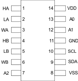
Pin Functions
| PIN | I/O | DESCRIPTION | |
|---|---|---|---|
| NAME | NO. | ||
| HA | 1 | I/O | High pin of potentiometer A |
| LA | 2 | I/O | Low pin of potentiometer A |
| WA | 3 | I/O | Wiper pin of potentiometer A |
| HB | 4 | I/O | High pin of potentiometer B |
| LB | 5 | I/O | Low pin of potentiometer B |
| WB | 6 | I/O | Wiper pin of potentiometer B |
| A2 | 7 | I | Address bit 2 |
| VSS | 8 | Power | Negative or GND power supply pin |
| SDA | 9 | I/O | I2C data I/O |
| SCL | 10 | I | I2C clock input |
| GND | 11 | — | Ground |
| A1 | 12 | I | Address bit 1 |
| A0 | 13 | I | Address bit 0 |
| VDD | 14 | Power | Positive power supply pin |