SNAS681A February 2017 – September 2021 TPL5110-Q1
PRODUCTION DATA
- 1 Features
- 2 Applications
- 3 Description
- 4 Revision History
- 5 Pin Configuration and Functions
- 6 Specifications
- 7 Detailed Description
- 8 Application and Implementation
- 9 Power Supply Recommendations
- 10Layout
- 11Device and Documentation Support
- 12Mechanical, Packaging, and Orderable Information
Package Options
Mechanical Data (Package|Pins)
- DDC|6
Thermal pad, mechanical data (Package|Pins)
Orderable Information
5 Pin Configuration and Functions
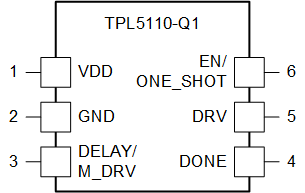
 Figure 5-1 SOT-236-Lead DDCTop View
Table 5-1 Pin Functions
| PIN | TYPE(1) | DESCRIPTION | APPLICATION INFORMATION | |
|---|---|---|---|---|
| NO. | NAME | |||
| 1 | VDD | P | Supply voltage | |
| 2 | GND | G | Ground | |
| 3 | DELAY/ M_DRV | I | Time interval set and manual MOSFET Power ON | Resistance between this pin and GND is used to select the time interval. The manual MOSFET power ON switch is also connected to this pin. |
| 4 | DONE | I | Logic Input for watchdog functionality | Digital signal driven by the µC to indicate successful processing. |
| 5 | DRV | O | Power Gating output signal generated every tIP | The Gate of the MOSFET is connected to this pin. When DRV = LOW, the MOSFET is ON. |
| 6 | EN/ ONE_SHOT | I | Selector of mode of operation | When EN/ONE_SHOT = HIGH, the TPL5110-Q1 works as a TIMER. When EN/ONE_SHOT = LOW, the TPL5110-Q1 turns on the MOSFET one time for the programmed time interval. The next power on of the MOSFET is enabled by the manual power ON. |
(1) G= Ground, P= Power, O= Output, I= Input.