SNAS681A February   2017  – September 2021 TPL5110-Q1

PRODUCTION DATA  

  1. Features
  2. Applications
  3. Description
  4. Revision History
  5. Pin Configuration and Functions
  6. Specifications
    1. 6.1 Absolute Maximum Ratings
    2. 6.2 ESD Ratings
    3. 6.3 Recommended Operating Ratings
    4. 6.4 Thermal Information
    5. 6.5 Electrical Characteristics
    6. 6.6 Timing Requirements
    7. 6.7 Typical Characteristics
  7. Detailed Description
    1. 7.1 Overview
    2. 7.2 Functional Block Diagram
    3. 7.3 Feature Description
      1. 7.3.1 DRV
      2. 7.3.2 DONE
    4. 7.4 Device Functional Modes
      1. 7.4.1 Start-Up
      2. 7.4.2 Timer Mode
      3. 7.4.3 One-Shot Mode
    5. 7.5 Programming
      1. 7.5.1 Configuring the Time Interval with the DELAY/M_DRV Pin
      2. 7.5.2 Manual MOSFET Power ON Applied to the DELAY/M_DRV Pin
        1. 7.5.2.1 DELAY/M_DRV
        2. 7.5.2.2 Circuitry
      3. 7.5.3 Selection of the External Resistance
      4. 7.5.4 Quantization Error
      5. 7.5.5 Error Due to Real External Resistance
  8. Application and Implementation
    1. 8.1 Application Information
    2. 8.2 Typical Application
      1. 8.2.1 Design Requirements
      2. 8.2.2 Detailed Design Procedure
      3. 8.2.3 Application Curve
  9. Power Supply Recommendations
  10. 10Layout
    1. 10.1 Layout Guidelines
    2. 10.2 Layout Example
  11. 11Device and Documentation Support
    1. 11.1 Receiving Notification of Documentation Updates
    2. 11.2 Support Resources
    3. 11.3 Trademarks
    4. 11.4 Electrostatic Discharge Caution
    5. 11.5 Glossary
  12. 12Mechanical, Packaging, and Orderable Information

Package Options

Mechanical Data (Package|Pins)
Thermal pad, mechanical data (Package|Pins)
Orderable Information

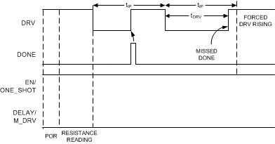
Start-Up

During start-up, after POR, the TPL5110-Q1 executes a one-time measurement of the resistance attached to the DELAY/M_DRV pin in order to determine the desired time interval for DRV. This measurement interval is tR_EXT. During this measurement a constant current is temporarily flowing into REXT.

Once the reading of the external resistance is completed the TPL5110-Q1 enters automatically in one of the 2 modes according to the EN/ONE_SHOT value. The EN/ONE_SHOT pin must be hard wired to GND or VDD according to the required mode of operation.
GUID-14DE7380-07FE-4F09-8425-DA8E1B1FE749-low.gifFigure 7-1 Start-Up - Timer Mode