SLVSCC6A March 2014 – June 2014 TPS2561A-Q1
PRODUCTION DATA.
- 1 Features
- 2 Applications
- 3 Description
- 4 Revision History
- 5 Device Comparison Table
- 6 Pin Functions and Configurations
- 7 Specifications
- 8 Parameter Measurement Information
- 9 Detailed Description
-
10Application and Implementation
- 10.1 Application Information
- 10.2
Typical Application
- 10.2.1
Design Current Limit
- 10.2.1.1 Design Requirements
- 10.2.1.2
Detailed Design Procedure
- 10.2.1.2.1 Determine Design Parameters
- 10.2.1.2.2 Programming the Current-Limit Threshold
- 10.2.1.2.3 Designing Above a Minimum Current Limit
- 10.2.1.2.4 Designing Below a Maximum Current Limit
- 10.2.1.2.5 Accounting for Resistor Tolerance
- 10.2.1.2.6 Power Dissipation and Junction Temperature
- 10.2.1.2.7 Auto-Retry Functionality
- 10.2.1.2.8 Two-Level Current-Limit Circuit
- 10.2.2 Application Curves
- 10.2.1
Design Current Limit
- 11Power Supply Requirements
- 12Layout
- 13Device and Documentation Support
- 14Mechanical, Packaging, and Orderable Information
Package Options
Mechanical Data (Package|Pins)
- DRC|10
Thermal pad, mechanical data (Package|Pins)
- DRC|10
Orderable Information
10 Application and Implementation
10.1 Application Information
The device is current-limited, power-distribution switch. It would limit the output current to IOS when short circuits or heavy capacitive loads are encountered.
10.2 Typical Application
10.2.1 Design Current Limit
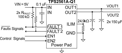 Figure 12. Typical Characteristics Reference Schematic
10.2.1.1 Design Requirements
For this design example, use the following as the input parameters.
Table 1. Design Parameters
| DESIGN PARAMTER | EXAMPLE VALUE |
|---|---|
| Input voltage | 5V |
| Minimum current limit | 2A |
| Maximum current limit | 1A |
10.2.1.2 Detailed Design Procedure
10.2.1.2.1 Determine Design Parameters
Beginning the design process requires deciding on a few parameters. The designer must know the following:
- Input voltage
- Minimum current limit
- Maximum current limit
10.2.1.2.2 Programming the Current-Limit Threshold
The overcurrent threshold is user programmable via an external resistor, RILIM. RILIM sets the current-limit threshold for both channels. The TPS2561A-Q1 use an internal regulation loop to provide a regulated voltage on the ILIM pin. The current-limit threshold is proportional to the current sourced out of ILIM. The recommended 1% resistor range for RILIM is 20 kΩ ≤ RILIM ≤ 187 kΩ to ensure stability of the internal regulation loop. Many applications require that the minimum current limit is above a certain current level or that the maximum current limit is below a certain current level, so it is important to consider the tolerance of the overcurrent threshold when selecting a value for RILIM. The following equations calculates the resulting overcurrent threshold for a given external resistor value (RILIM). The traces routing the RILIM resistor to the TPS2561A-Q1 should be as short as possible to reduce parasitic effects on the current-limit accuracy.
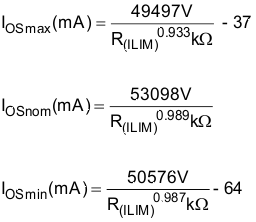
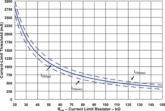 Figure 13. Current-Limit Threshold vs. RILIM
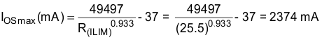
10.2.1.2.3 Designing Above a Minimum Current Limit
Some applications require that current limiting cannot occur below a certain threshold. For this example, assume that 2 A must be delivered to the load so that the minimum desired current-limit threshold is 2000 mA. Use the IOS equations and Figure 13 to select RILIM.
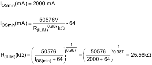
Select the closest 1% resistor less than the calculated value: RILIM = 25.5 kΩ. This sets the minimum current-limit threshold at 2005 mA .
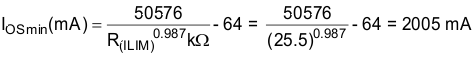
Use the IOS equations, Figure 13, and the previously calculated value for RILIM to calculate the maximum resulting current-limit threshold at 2374 mA.
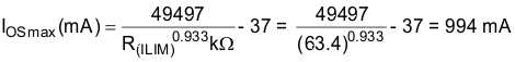
10.2.1.2.4 Designing Below a Maximum Current Limit
Some applications require that current limiting must occur below a certain threshold. For this example, assume that 1 A must be delivered to the load so that the minimum desired current-limit threshold is 1000 mA. Use the IOS equations and Figure 13 to select RILIM.
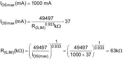
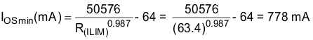
Select the closest 1% resistor greater than the calculated value: RILIM = 63.4 kΩ. This sets the maximum current-limit threshold at 994 A.
Use the IOS equations, Figure 13, and the previously calculated value for RILIM to calculate the minimum resulting current-limit threshold at 778 mA.
10.2.1.2.5 Accounting for Resistor Tolerance
The previous sections described the selection of RILIM given certain application requirements and the importance of understanding the current-limit threshold tolerance. The analysis focused only on the TPS2561A-Q1 performance and assumed an exact resistor value. However, resistors sold in quantity are not exact and are bounded by an upper and lower tolerance centered around a nominal resistance. The additional RILIM resistance tolerance directly affects the current-limit threshold accuracy at a system level. The following table shows a process that accounts for worst-case resistor tolerance assuming 1% resistor values. Step one follows the selection process outlined in the application examples above. Step two determines the upper and lower resistance bounds of the selected resistor. Step three uses the upper and lower resistor bounds in the IOS equations to calculate the threshold limits. It is important to use tighter tolerance resistors, that is, 0.5% or 0.1%, when precision current limiting is desired.
Table 2. Common RILIM Resistor Selections
| Desired Nominal Current Limit (mA) | Ideal Resistor (kΩ) | Closest 1% Resistor (kΩ) | Resistor Tolerance | Actual Limits | |||||
|---|---|---|---|---|---|---|---|---|---|
| 1% low (kΩ) | 1% high (kΩ) | IOS MIN (mA) | IOS Nom (mA) | IOS MAX (mA) | |||||
| 300 | 187.5 | 187 | 185.1 | 188.9 | 223 | 301 | 342 | ||
| 550 | 101.6 | 102 | 101.0 | 103.0 | 457 | 548 | 631 | ||
| 800 | 69.5 | 69.8 | 69.1 | 70.5 | 694 | 797 | 914 | ||
| 1050 | 52.8 | 52.3 | 51.8 | 52.8 | 944 | 1060 | 1208 | ||
| 1300 | 42.6 | 42.2 | 41.8 | 42.6 | 1182 | 1311 | 1484 | ||
| 1550 | 35.6 | 35.7 | 35.3 | 36.1 | 1406 | 1547 | 1741 | ||
| 1800 | 30.6 | 30.9 | 30.6 | 31.2 | 1631 | 1784 | 1998 | ||
| 2050 | 26.9 | 26.7 | 26.4 | 27.0 | 1894 | 2062 | 2295 | ||
| 2300 | 23.9 | 23.7 | 23.5 | 23.9 | 2138 | 2320 | 2569 | ||
| 2550 | 21.5 | 21.5 | 21.3 | 21.7 | 2360 | 2554 | 2817 | ||
| 2800 | 19.6 | 19.6 | 19.4 | 19.8 | 2592 | 2799 | 3075 | ||
10.2.1.2.6 Power Dissipation and Junction Temperature
The low on-resistance of the N-channel MOSFET allows small surface-mount packages to pass large currents. It is good design practice to estimate power dissipation and junction temperature. The below analysis gives an approximation for calculating junction temperature based on the power dissipation in the package. However, it is important to note that thermal analysis is strongly dependent on additional system level factors. Such factors include air flow, board layout, copper thickness and surface area, and proximity to other devices dissipating power. Good thermal design practice must include all system level factors in addition to individual component analysis.
Begin by determining the rDS(on) of the N-channel MOSFET relative to the input voltage and operating temperature. As an initial estimate, use the highest operating ambient temperature of interest and read RDS(on) from the typical characteristics graph. Using this value, the power dissipation can be calculated by:
PD = (RDS(on) × IOUT12) +(RDS(on) × IOUT22)
Where:
PD = Total power dissipation (W)
rDS(on) = Power switch on-resistance of one channel (Ω)
IOUTx = Maximum current-limit threshold set by RILIM(A)
This step calculates the total power dissipation of the N-channel MOSFET.
Finally, calculate the junction temperature:
TJ = PD × θJA + TA
Where:
TA = Ambient temperature (°C)
θJA = Thermal resistance (°C/W)
PD = Total power dissipation (W)
Compare the calculated junction temperature with the initial estimate. If they are not within a few degrees, repeat the calculation using the "refined" RDS(on) from the previous calculation as the new estimate. Two or three iterations are generally sufficient to achieve the desired result. The final junction temperature is highly dependent on thermal resistance θJA, and thermal resistance is highly dependent on the individual package and board layout. The Thermal Characteristics Table provides example thermal resistances for specific packages and board layouts.
10.2.1.2.7 Auto-Retry Functionality
Some applications require that an overcurrent condition disables the part momentarily during a fault condition and re-enables after a pre-set time. This auto-retry functionality can be implemented with an external resistor and capacitor. During a fault condition, FAULTx pulls ENx low disabling the part. The part is disabled when ENx is pulled below the turn-off threshold, and FAULTx goes high impedance allowing CRETRY to begin charging. The part re-enables when the voltage on ENx reaches the turn-on threshold, and the auto-retry time is determined by the resistor, capacitor time constant. The part will continue to cycle in this manner until the fault condition is removed.
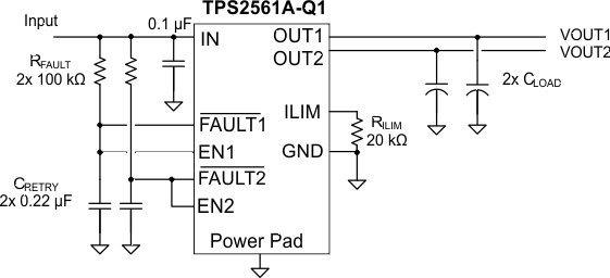 Figure 14. Auto-Retry Functionality
Some applications require auto-retry functionality and the ability to enable/disable with an external logic signal. The figure below shows how an external logic signal can drive EN through RFAULT and maintain auto-retry functionality. The resistor/capacitor time constant determines the auto-retry time-out period.
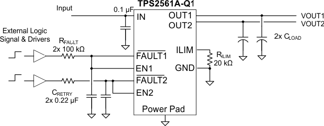 Figure 15. Auto-Retry Functionality With External EN Signal
10.2.1.2.8 Two-Level Current-Limit Circuit
Some applications require different current-limit thresholds depending on external system conditions. Figure 16 shows an implementation for an externally controlled, two-level current-limit circuit. The current-limit threshold is set by the total resistance from ILIM to GND (see previously discussed Programming the Current-Limit Threshold section). A logic-level input enables/disables MOSFET Q1 and changes the current-limit threshold by modifying the total resistance from ILIM to GND. Additional MOSFET/resistor combinations can be used in parallel to Q1/R2 to increase the number of additional current-limit levels.
NOTE
ILIM should never be driven directly with an external signal.
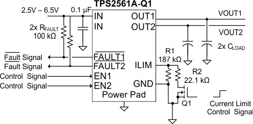 Figure 16. Two-Level Current-Limit Circuit
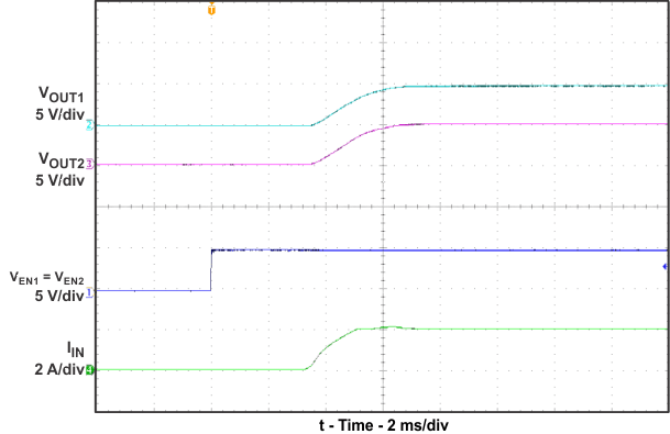
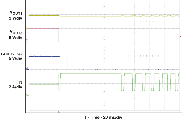
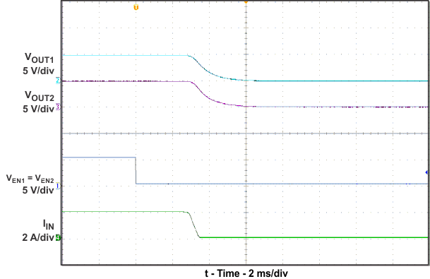
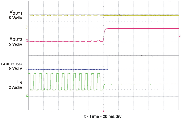
10.2.2 Application Curves