SLVSA23A September 2009 – January 2024 TPS5410-Q1
PRODUCTION DATA
- 1
- 1Features
- 2Applications
- 3Description
- 4Electrostatic Discharge Caution
- 5Ordering Information
- 6Pin Assignments
- 7Specifications
-
8Application Information
- 8.1 Functional Block Diagram
- 8.2
Detailed Description
- 8.2.1 Oscillator Frequency
- 8.2.2 Voltage Reference
- 8.2.3 Enable (ENA) and Internal Slow Start
- 8.2.4 Undervoltage Lockout (UVLO)
- 8.2.5 Boost Capacitor (BOOT)
- 8.2.6 Output Feedback (VSENSE)
- 8.2.7 Internal Compensation
- 8.2.8 Voltage Feed Forward
- 8.2.9 Pulse-Width-Modulation (PWM) Control
- 8.2.10 Overcurrent Liming
- 8.2.11 Overvoltage Protection
- 8.2.12 Thermal Shutdown
- 8.2.13 PCB Layout
- 8.2.14 Application Circuits
- 8.2.15 Design Procedure
- 8.2.16 Output Filter Capacitor Selection
- 8.2.17 External Compensation Network
- 8.3 Advanced Information
- 8.4 Performance Graphs
- 8.5 Performance Graphs
- 9Revision History
Package Options
Mechanical Data (Package|Pins)
- D|8
Thermal pad, mechanical data (Package|Pins)
Orderable Information
8.2.17 External Compensation Network
When using ceramic output capacitors, additional circuitry is required to stabilize the closed loop system. For this circuit the external components are R3, C5, C6 and C7. To determine the value of these components, first calculate the LC resonant frequency of the output filter:
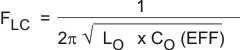
For this example the effective resonant frequency is calculated as 2306 Hz
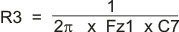
The network composed of R1, R2, R3, C5, C6 and C7 has two poles and two zeros that are used to tailor the overall response of the feedback network to accommodate the use of the ceramic output capacitors. The pole and zero locations are given by the following equations:
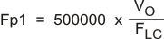


The final pole is located at a frequency too high to be of concern. The values for R1 and R2 are fixed by the 5-V output voltage as calculated using Equation 12. Now the values of R3, C5, C6 and C7 are determined using Equation 18, Equation 19, and Equation 20:
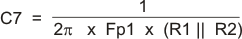
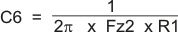
For this design, using the closest standard values, C7 is 0.056 μF, R3 is 1.76 kΩ and C6 is 2700 pF. C5 is added to improve load regulation performance. It is effectively in parallel with C6 in the location of the second pole frequency, so it should be small in relationship to C6. C5 should be less the 1/10 the value of C6. For this example, 150 pF works well.
For additional information on external compensation of the TPS5410 or other wide voltage range SWIFT devices, see SLVA237 Using TPS5410/20/30/31 With Aluminum/Ceramic Output Capacitors.