SLVSA23A September 2009 – January 2024 TPS5410-Q1
PRODUCTION DATA
- 1
- 1Features
- 2Applications
- 3Description
- 4Electrostatic Discharge Caution
- 5Ordering Information
- 6Pin Assignments
- 7Specifications
-
8Application Information
- 8.1 Functional Block Diagram
- 8.2
Detailed Description
- 8.2.1 Oscillator Frequency
- 8.2.2 Voltage Reference
- 8.2.3 Enable (ENA) and Internal Slow Start
- 8.2.4 Undervoltage Lockout (UVLO)
- 8.2.5 Boost Capacitor (BOOT)
- 8.2.6 Output Feedback (VSENSE)
- 8.2.7 Internal Compensation
- 8.2.8 Voltage Feed Forward
- 8.2.9 Pulse-Width-Modulation (PWM) Control
- 8.2.10 Overcurrent Liming
- 8.2.11 Overvoltage Protection
- 8.2.12 Thermal Shutdown
- 8.2.13 PCB Layout
- 8.2.14 Application Circuits
- 8.2.15 Design Procedure
- 8.2.16 Output Filter Capacitor Selection
- 8.2.17 External Compensation Network
- 8.3 Advanced Information
- 8.4 Performance Graphs
- 8.5 Performance Graphs
- 9Revision History
Package Options
Mechanical Data (Package|Pins)
- D|8
Thermal pad, mechanical data (Package|Pins)
Orderable Information
8.2.8 Voltage Feed Forward
The internal voltage feed forward provides a constant DC power stage gain despite any variations with the input voltage. This greatly simplifies the stability analysis and improves the transient response. Voltage feed forward varies the peak ramp voltage inversely with the input voltage so that the modulator and power stage gain are constant at the feed forward gain, i.e.
Equation 1. 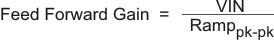
The typical feed forward gain of TPS5410 is 25.