SLVSA23A September 2009 – January 2024 TPS5410-Q1
PRODUCTION DATA
- 1
- 1Features
- 2Applications
- 3Description
- 4Electrostatic Discharge Caution
- 5Ordering Information
- 6Pin Assignments
- 7Specifications
-
8Application Information
- 8.1 Functional Block Diagram
- 8.2
Detailed Description
- 8.2.1 Oscillator Frequency
- 8.2.2 Voltage Reference
- 8.2.3 Enable (ENA) and Internal Slow Start
- 8.2.4 Undervoltage Lockout (UVLO)
- 8.2.5 Boost Capacitor (BOOT)
- 8.2.6 Output Feedback (VSENSE)
- 8.2.7 Internal Compensation
- 8.2.8 Voltage Feed Forward
- 8.2.9 Pulse-Width-Modulation (PWM) Control
- 8.2.10 Overcurrent Liming
- 8.2.11 Overvoltage Protection
- 8.2.12 Thermal Shutdown
- 8.2.13 PCB Layout
- 8.2.14 Application Circuits
- 8.2.15 Design Procedure
- 8.2.16 Output Filter Capacitor Selection
- 8.2.17 External Compensation Network
- 8.3 Advanced Information
- 8.4 Performance Graphs
- 8.5 Performance Graphs
- 9Revision History
Package Options
Mechanical Data (Package|Pins)
- D|8
Thermal pad, mechanical data (Package|Pins)
Orderable Information
8.5 Performance Graphs
The performance graphs in Figure 8-13 - Figure 8-18 are applicable to the circuit in Figure 8-4. TA = 25 °C. unless otherwise specified.
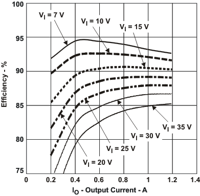 Figure 8-13 Efficiency vs. Output Current
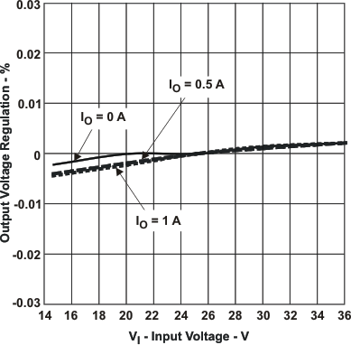 Figure 8-15 Output Voltage Regulation % vs. Input Voltage
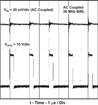 Figure 8-17 Output Voltage Ripple and PH Node, IO = 1 A
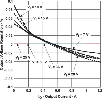 Figure 8-14 Output Voltage Regulation % vs. Output Current
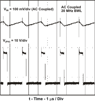 Figure 8-16 Input Voltage Ripple and PH Node, IO = 1 A
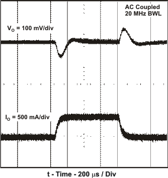 Figure 8-18 Transient Response, IO Step 0.25 to 0.75 A