SLVSC33A August 2013 – October 2022 TPS54625
PRODUCTION DATA
- 1 FEATURES
- 2 APPLICATIONS
- 3 DESCRIPTION
- 4 ORDERING INFORMATION (1)
- 5 ABSOLUTE MAXIMUM RATINGS
- 6 THERMAL INFORMATION
- 7 RECOMMENDED OPERATING CONDITIONS
- 8 ELECTRICAL CHARACTERISTICS
- 9 DEVICE INFORMATION
- 10OVERVIEW
- 11DETAILED DESCRIPTION
- 12TYPICAL CHARACTERISTICS
- 13DESIGN GUIDE
- 14THERMAL INFORMATION
- 15LAYOUT CONSIDERATIONS
- 16Revision History
Package Options
Mechanical Data (Package|Pins)
- PWP|14
Thermal pad, mechanical data (Package|Pins)
- PWP|14
Orderable Information
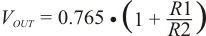
13.2 Output Voltage Resistors Selection
The output voltage is set with a resistor divider from the output node to the VFB pin. It is recommended to use 1% tolerance or better divider resistors. Start by using Equation 2 to calculate VOUT.
To improve efficiency at very light loads consider using larger value resistors, too high of resistance will be more susceptible to noise and voltage errors from the VFB input current will be more noticeable.
Equation 2.