SLVSC33A August 2013 – October 2022 TPS54625
PRODUCTION DATA
- 1 FEATURES
- 2 APPLICATIONS
- 3 DESCRIPTION
- 4 ORDERING INFORMATION (1)
- 5 ABSOLUTE MAXIMUM RATINGS
- 6 THERMAL INFORMATION
- 7 RECOMMENDED OPERATING CONDITIONS
- 8 ELECTRICAL CHARACTERISTICS
- 9 DEVICE INFORMATION
- 10OVERVIEW
- 11DETAILED DESCRIPTION
- 12TYPICAL CHARACTERISTICS
- 13DESIGN GUIDE
- 14THERMAL INFORMATION
- 15LAYOUT CONSIDERATIONS
- 16Revision History
Package Options
Mechanical Data (Package|Pins)
- PWP|14
Thermal pad, mechanical data (Package|Pins)
- PWP|14
Orderable Information
15 LAYOUT CONSIDERATIONS
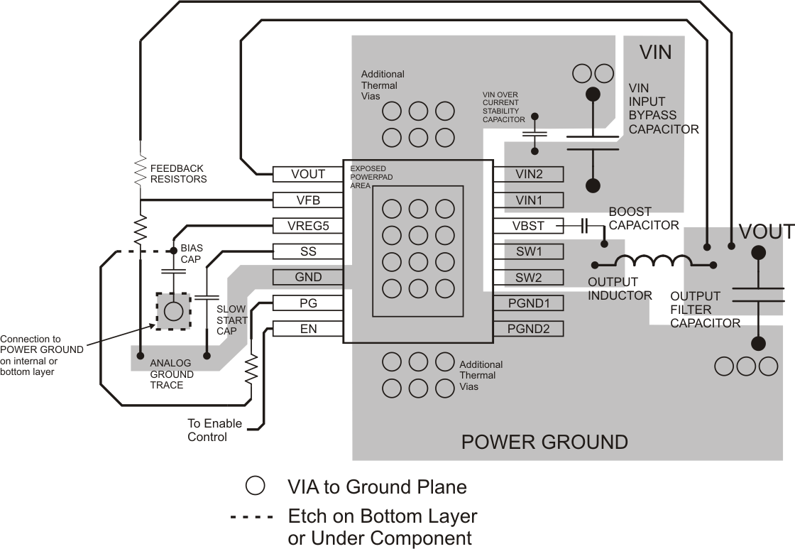
- A top side area should be filled with ground as much as possible due to relatively higher current output device.
- The ground area under the device thermal pad should be large as possible and directly connect to the thermal pad. Also 2nd, 3rd and 4th PCB layer should be connected to ground directly from the thermal pad.
- Keep the input switching current loop as small as possible.
- Keep the SW node as physically small and short as possible to minimize parasitic capacitance and inductance and to minimize radiated emissions. Kelvin connections should be brought from the output to the feedback pin of the device.
- Keep analog and non-switching components away from switching components.
- Make a single point connection from the signal ground to power ground.
- Do not allow switching current to flow under the device.
- Keep the pattern lines for VIN and PGND broad.
- Exposed pad of device must be connected to PGND with solder.
- VREG5 capacitor should be placed near the device, and connected PGND.
- Output capacitor should be connected to a broad pattern of the PGND.
- Voltage feedback loop should be as short as possible, and preferably with ground shield.
- Lower resistor of the voltage divider which is connected to the VFB pin should be tied to SGND.
- Providing sufficient via is preferable for VIN, SW and PGND connection.
- PCB pattern for VIN, SW, and PGND should be as broad as possible.
- VIN Capacitor should be placed as near as possible to the device.
 Figure 15-1 PCB Layout