SLVSBF3B June 2012 – May 2019 TPS54678
PRODUCTION DATA.
- 1 Features
- 2 Applications
- 3 Description
- 4 Revision History
- 5 Pin Configuration and Functions
- 6 Specifications
-
7 Detailed Description
- 7.1 Overview
- 7.2 Functional Block Diagram
- 7.3
Feature Description
- 7.3.1 Fixed Frequency PWM Control
- 7.3.2 Slope Compensation and Output Current
- 7.3.3 Bootstrap Voltage (Boot) and Low Dropout Operation
- 7.3.4 Error Amplifier
- 7.3.5 Voltage Reference
- 7.3.6 Adjusting the Output Voltage
- 7.3.7 Enable and Adjusting Undervoltage Lockout
- 7.3.8 Soft-Start Pin
- 7.3.9 Sequencing
- 7.3.10 Constant Switching Frequency and Timing Resistor (RT/CLK Pin)
- 7.3.11 Overcurrent Protection
- 7.3.12 Safe Start-Up into Prebiased Outputs
- 7.3.13 Synchronize Using the RT/CLK Pin
- 7.3.14 Power Good (PWRGD Pin)
- 7.3.15 Overvoltage Transient Protection
- 7.3.16 Thermal Shutdown
- 7.4 Device Functional Modes
-
8 Application and Implementation
- 8.1 Application Information
- 8.2
Typical Application
- 8.2.1 Design Requirements
- 8.2.2
Detailed Design Procedure
- 8.2.2.1 Custom Design With WEBENCH® Tools
- 8.2.2.2 Step One: Select the Switching Frequency
- 8.2.2.3 Step Two: Select the Output Inductor
- 8.2.2.4 Step Three: Choose the Output Capacitor
- 8.2.2.5 Step Four: Select the Input Capacitor
- 8.2.2.6 Step Five: Choose the Soft-Start Capacitor
- 8.2.2.7 Step Six: Select the Bootstrap Capacitor
- 8.2.2.8 Step Eight: Select Output Voltage and Feedback Resistors
- 8.2.2.9 Step Nine: Select Loop Compensation Components
- 8.2.3 Application Curves
- 9 Power Supply Recommendations
- 10Layout
- 11Device and Documentation Support
- 12Mechanical, Packaging, and Orderable Information
Package Options
Mechanical Data (Package|Pins)
- RTE|16
Thermal pad, mechanical data (Package|Pins)
- RTE|16
Orderable Information
7.3.9 Sequencing
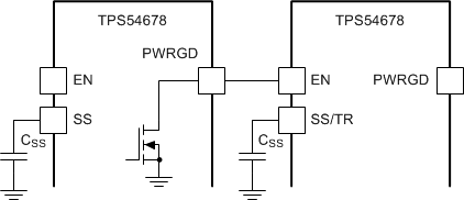
Many of the common power supply sequencing methods can be implemented using the SS/TR, EN and PWRGD pins. The sequential method can be implemented using an open-drain or collector output of a power on reset pin of another device. The sequential method is shown in Figure 23. The power good is coupled to the EN pin on the TPS54678, which will enable the second power supply once the primary supply reaches regulation.
 Figure 23. Sequential Start-Up Sequence