SLVSBF3B June 2012 – May 2019 TPS54678
PRODUCTION DATA.
- 1 Features
- 2 Applications
- 3 Description
- 4 Revision History
- 5 Pin Configuration and Functions
- 6 Specifications
-
7 Detailed Description
- 7.1 Overview
- 7.2 Functional Block Diagram
- 7.3
Feature Description
- 7.3.1 Fixed Frequency PWM Control
- 7.3.2 Slope Compensation and Output Current
- 7.3.3 Bootstrap Voltage (Boot) and Low Dropout Operation
- 7.3.4 Error Amplifier
- 7.3.5 Voltage Reference
- 7.3.6 Adjusting the Output Voltage
- 7.3.7 Enable and Adjusting Undervoltage Lockout
- 7.3.8 Soft-Start Pin
- 7.3.9 Sequencing
- 7.3.10 Constant Switching Frequency and Timing Resistor (RT/CLK Pin)
- 7.3.11 Overcurrent Protection
- 7.3.12 Safe Start-Up into Prebiased Outputs
- 7.3.13 Synchronize Using the RT/CLK Pin
- 7.3.14 Power Good (PWRGD Pin)
- 7.3.15 Overvoltage Transient Protection
- 7.3.16 Thermal Shutdown
- 7.4 Device Functional Modes
-
8 Application and Implementation
- 8.1 Application Information
- 8.2
Typical Application
- 8.2.1 Design Requirements
- 8.2.2
Detailed Design Procedure
- 8.2.2.1 Custom Design With WEBENCH® Tools
- 8.2.2.2 Step One: Select the Switching Frequency
- 8.2.2.3 Step Two: Select the Output Inductor
- 8.2.2.4 Step Three: Choose the Output Capacitor
- 8.2.2.5 Step Four: Select the Input Capacitor
- 8.2.2.6 Step Five: Choose the Soft-Start Capacitor
- 8.2.2.7 Step Six: Select the Bootstrap Capacitor
- 8.2.2.8 Step Eight: Select Output Voltage and Feedback Resistors
- 8.2.2.9 Step Nine: Select Loop Compensation Components
- 8.2.3 Application Curves
- 9 Power Supply Recommendations
- 10Layout
- 11Device and Documentation Support
- 12Mechanical, Packaging, and Orderable Information
Package Options
Mechanical Data (Package|Pins)
- RTE|16
Thermal pad, mechanical data (Package|Pins)
- RTE|16
Orderable Information
8.2.2.9 Step Nine: Select Loop Compensation Components
There are several possible methods to design closed-loop compensation for DC/DC converters. For the ideal current mode control, the design equations can be easily simplified. The power stage gain is constant at low frequencies, and rolls off at –20 dB/decade above the modulator pole frequency. The power stage phase is zero degrees at low frequencies and starts to fall one decade below the modulator pole frequency reaching a minimum of –90 degrees one decade above the modulator pole frequency. In this case the modulator pole is a simple pole shown in Equation 29.

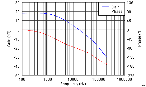
For the TPS54678 most circuits will have relatively high amounts of slope compensation. As more slope compensation is applied, the power stage characteristics will deviate from the ideal approximations. The phase loss of the power stage will extend beyond –90 degrees and can approach –180 degrees, making compensation more difficult. The power stage transfer function can be solved but it is a tedious hand calculation that does not lend itself to simple approximations. It is easier to either simulate the circuit or to actually measure the plant transfer function so that a reliable compensation circuit can be designed. The latter technique used in this design procedure. The power stage plant was measured and is shown in Figure 31.
 Figure 31. Measured Plant Bode
 For this design, the desired crossover frequency Fc is 50 kHz. From the power stage gain and phase plot above, the gain at 50 kHz is –10.6 dB and the phase is –123.3 degrees. Because the plant phase loss is greater than –90 degrees, to achieve at least 60 degrees of phase margin, additional phase boost from a feedforward capacitor in parallel with the upper resistor of the voltage set point divider is required.
See the schematic in Figure 30. R3 sets the gain of the compensated error amplifier to be equal and opposite (in dB) to the power stage gain at Fc, so 10.6 dB is needed. The required value of R3 can be calculated from Equation 30.

The compensator zero formed by R3 and C6 is placed at the plant pole, as shown approximately 2.5 kHz. The required value for C6 is given by Equation 31.

The high-frequency noise pole formed by C5 and R3 is not used in this design. If the resulting design shows noise susceptibility, the value of C5 can be calculated per Equation 32.

To avoid a penalty in loop phase, the Fpole in Equation 32 should be placed a decade above Fc or higher, and is intended to reject noise at FSW.
The feedforward capacitor C15 is used to increase the phase boost at crossover above what is normally available from Type II compensation. It places an additional zero/pole pair with the zero located at Equation 33 and the pole at Equation 34.


This zero and pole pair is not independent since R9 and R10 are set by the desired VOUT. Once the zero location is chosen, the pole is fixed as well. For optimum performance, the zero and pole should be located symmetrically about the intended crossover frequency. The required value for C15 can be calculated from Equation 35.

Table 2 lists the values the compensation equations yield.
Table 2. Frequency Compensation Component Values
| REF DES | CALCULATED VALUE | CHOSEN VALUE |
|---|---|---|
| R3 | 19.6 kΩ | 26.7 kΩ |
| C6 | 2.38 nF | 2.2 nF |
| C15 | 225 pF | 150 pF |